Automotive High Current LED Controller
A6265
6
Allegro MicroSystems, LLC
115 Northeast Cutoff
Worcester, Massachusetts 01615-0036 U.S.A.
1.508.853.5000; www.allegromicro.com
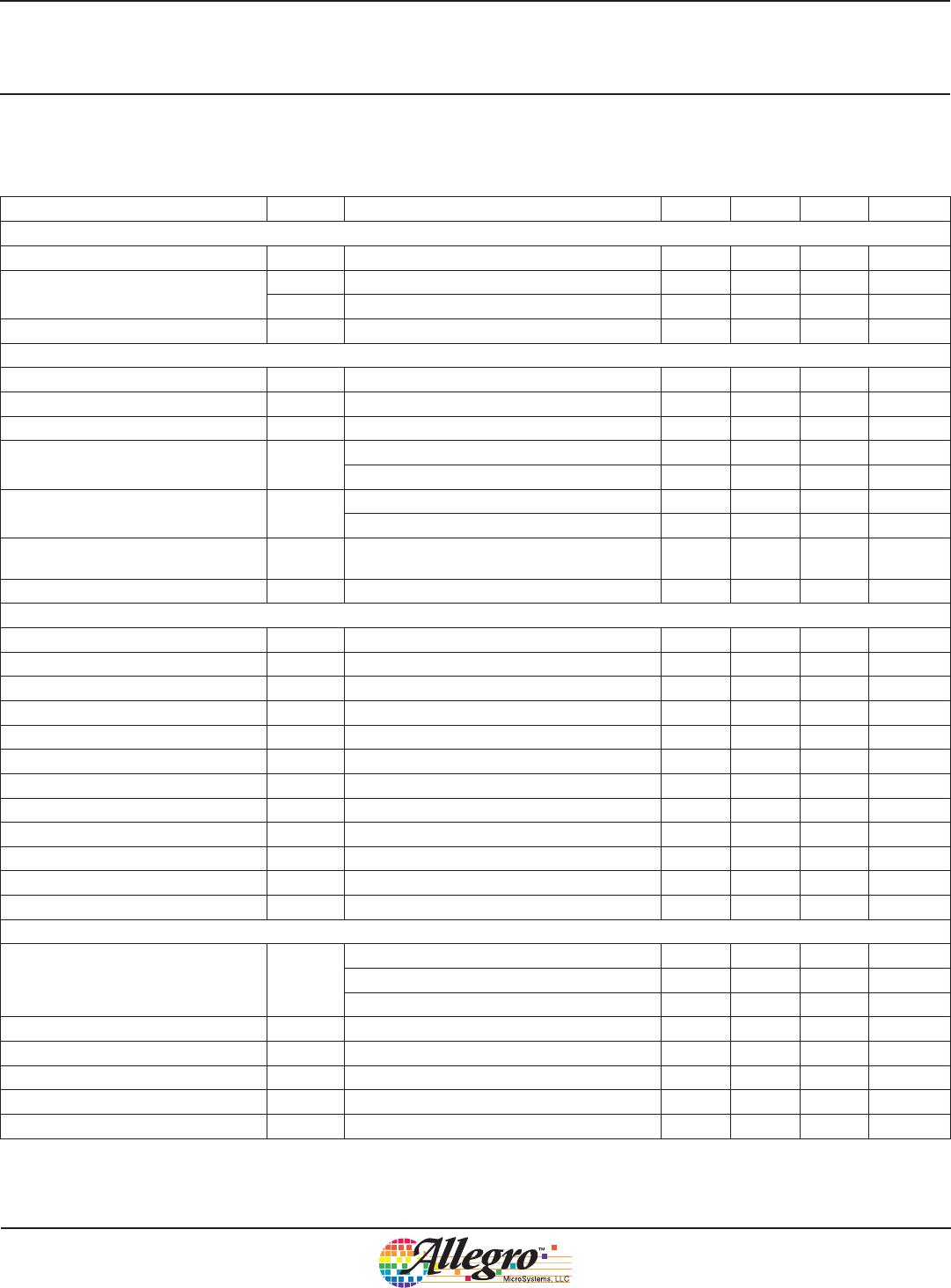
ELECTRICAL CHARACTERISTICS
1
(continued) Valid at T
J
= –40°C to 150°C, V
IN
= 8 to 40 V; unless otherwise noted
Characteristics Symbol Test Conditions Min. Typ. Max. Unit
Oscillator (continued)
OSC Input Hysteresis V
Oihys
300 600 – mV
OSC Watchdog Period t
OSWD
Between successive rising edges 7 – – s
CKOUT Output High Voltage V
COH
I
OH
= –1 mA V
REG
– 1 – V
REG
V
CKOUT Output Low Voltage V
COL
I
OL
= 1 mA – – 0.4 V
LED Current Sense
Input Bias Current LN (BB mode)
4
I
LN
LP = LN = VIN – 6 – A
Input Bias Current LP (BB mode)
4
I
LP
LP = LN = VIN – 220 – A
Input Bias Current LN (B mode)
4
I
LN
LP = LN = 0 V – –2 – A
Input Bias Current LP (B mode)
4
I
LP
LP = LN = 0 V – –25 – A
Differential Input Voltage (Active) V
IDL
EN = High, V
IDL
= V
LP
– V
LN
– 100 – mV
Differential Input Voltage (PWM off) V
IDLO
EN = Low, V
IDL
= V
LP
– V
LN
– 8 – mV
Input Common-Mode Range (BB mode)
4
V
CMLH
V
LP
= V
LN
V
IN
–V
IN
+ 1 V
Input Common-Mode Range (B mode)
4
V
CMLL
V
LP
= V
LN
0 – 1 V
Current Error E
ISL
[(10 × I
LED
× R
SL
) – 1] × 100 –5 – 5 %
Switch Current Sense
Input Bias Current I
BIASS
SP = SN = 0 to 2 V –30 – – A
Maximum Differential Input Voltage
3
V
IDS
V
IDS
= V
SP
– V
SN
with D = 50% 330 410 490 mV
Input Source Current I
INS
V
IDS
= 400 mV – 400 – A
Input Common-Mode Range V
CMS
V
SP
= V
SN
0 – 2 V
Diagnostics and Protection
Fault Blank Timer
5
t
FB
Start-up – 3 – ms
VREG Undervoltage Turn-Off V
REGUV
Decreasing V
REG
4.1 4.3 4.5 V
VREG Undervoltage Hysteresis V
REGUVhys
130 150 160 mV
LED String Short Voltage V
SCL
430 505 580 mV
Non-Reference LED Short Offset
Voltage
V
SCO
160 200 240 mV
Reference LED Short Offset Voltage V
SCOR
430 505 580 mV
LED Open Voltage V
OCL
5 5.5 6 V
LF Bias Current (BB mode)
4
I
LF
LF = LA = VIN + 1.7 V – 46 – A
LA Bias Current (BB mode)
4
I
LA
LF = LA = VIN + 1.7 V – 170 – A
LF Bias Current (B mode)
4
I
LF
LF = 1.7 V – 8 – A
LA Bias Current (B mode)
4
I
LA
LA = 1.7 V – 34 – A
LED Undercurrent Voltage Difference
6
V
UCL
– 1 – mV
Open Fault Time-Out t
OTO
f
OSC
= 350 kHz – 94 – ms
Overtemperature Warning Threshold T
JF
Temperature increasing – 170 – ºC
Overtemperature Hysteresis T
Jhys
Recovery = T
JF
– T
Jhys
–15– ºC
1
For input and output current specifications, negative current is defined as coming out of (sourcing) the specified device pin.
2
Function is correct but parameters are not guaranteed below the general limit (8 V).
3
Parameters ensured by design.
4
BB mode = buck-boost (supply-referenced) mode, B mode = boost (ground-referenced) mode.
5
Fault Blank timer not enabled for open-LED condition.
6
Undercurrent when V
SENSEL
< V
IDL
– V
UCL
, where V
SENSEL
is the voltage across the LED current sense resistor R
SL
.