Information furnished by Analog Devices is believed to be accurate and
reliable. However, no responsibility is assumed by Analog Devices for its
use, nor for any infringements of patents or other rights of third parties
that may result from its use. No license is granted by implication or oth-
erwise under any patent or patent rights of Analog Devices. Trademarks
and registered trademarks are the property of their respective companies.
One Technology Way, P.O. Box 9106, Norwood, MA 02062-9106, U.S.A.
Tel: 781/329-4700 www.analog.com
Fax: 781/326-8703 © 2003 Analog Devices, Inc. All rights reserved.
AD831
Low Distortion Mixer
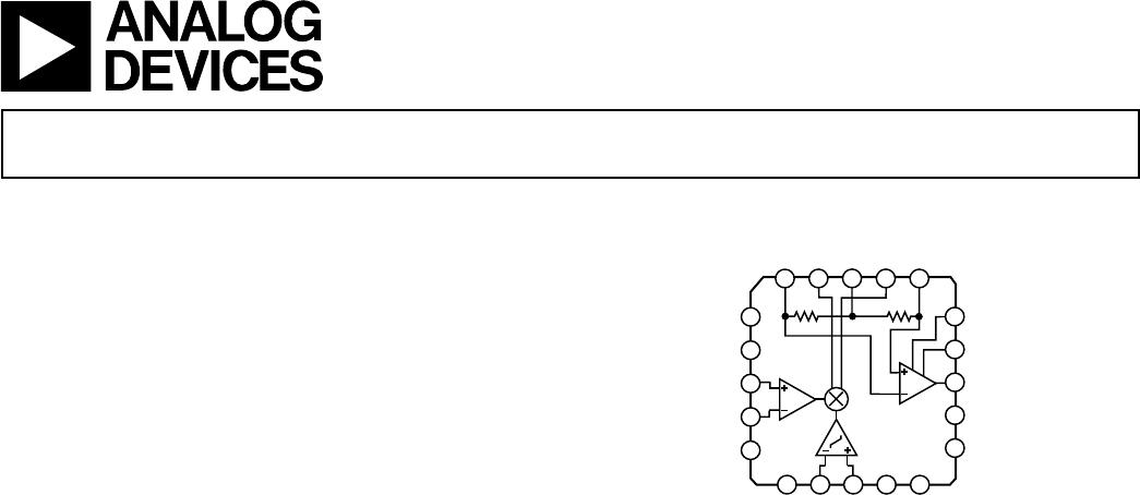
FUNCTIONAL BLOCK DIAGRAM
�
�
FEATURES
Doubly Balanced Mixer
Low Distortion
+24 dBm Third Order Intercept (IP3)
+10 dBm 1 dB Compression Point
Low LO Drive Required: –10 dBm
Bandwidth
500 MHz RF and LO Input Bandwidths
250 MHz Differential Current IF Output
DC to >200 MHz Single-Ended Voltage IF Output
Single- or Dual-Supply Operation
DC Coupled Using Dual Supplies
All Ports May Be DC Coupled
No Lower Frequency Limit—Operation to DC
User-Programmable Power Consumption
APPLICATIONS
High Performance RF/IF Mixer
Direct to Baseband Conversion
Image-Reject Mixers
I/Q Modulators and Demodulators
PRODUCT DESCRIPTION
The AD831 is a low distortion, wide dynamic range, monolithic
mixer for use in such applications as RF to IF downconversion
in HF and VHF receivers, the second mixer in DMR base sta-
tions, direct-to-baseband conversion, quadrature modulation and
demodulation, and doppler shift detection in ultrasound imaging
applications. The mixer includes an LO driver and a low noise
output amplier and provides both user-programmable power
consumption and third order intercept point.
The AD831 provides a +24 dBm third order intercept point for
–10 dBm LO power, thus improving system performance and
reducing system cost compared to passive mixers, by eliminating
the need for a high power LO driver and its attendant shielding
and isolation problems.
The RF, IF, and LO ports may be dc or ac coupled when the
mixer is operating from ±5 V supplies or ac coupled when oper-
ating from a single-supply of 9 V minimum. The mixer operates
with RF and LO inputs as high as 500 MHz.
The mixer’s IF output is available as either a differential current
output or a single-ended voltage output. The differential output is
from a pair of open collectors and may be ac coupled via a trans-
former or capacitor to provide a 250 MHz output bandwidth. In
downconversion applications, a single capacitor connected across
these outputs implements a low-pass lter to reduce harmonics
directly at the mixer core, simplifying output ltering. When
building a quadrature-amplitude modulator or image reject mixer,
the differential current outputs of two AD831s may be summed
by connecting them together.
An integral low noise amplier provides a single-ended voltage
output and can drive such low impedance loads as lters, 50
amplier inputs, and A/D converters. Its small signal bandwidth
exceeds 200 MHz. A single resistor connected between pins
OUT and FB sets its gain. The amplier’s low dc offset allows
its use in such direct-coupled applications as direct-to-baseband
conversion and quadrature-amplitude demodulation.
The mixer’s SSB noise gure is 10.3 dB at 70 MHz using its
output amplier and optimum source impedance. Unlike passive
mixers, the AD831 has no insertion loss and does not require an
external diplexer or passive termination.
A programmable-bias feature allows the user to reduce power
consumption, with a reduction in the 1 dB compression point and
third-order intercept. This permits a tradeoff between dynamic
range and power consumption. For example, the AD831 may be
used as a second mixer in cellular and two-way radio base stations
at reduced power while still providing a substantial performance
improvement over passive solutions.
PRODUCT HIGHLIGHTS
1. –10 dBm LO Drive for a +24 dBm Output Referred Third
Order Intercept Point
2. Single-Ended Voltage Output
3. High Port-to-Port Isolation
4. No Insertion Loss
5. Single- or Dual-Supply Operation
6. 10.3 dB Noise Figure
REV. C