–2–
AD831–SPECIFICATIONS
AD831
–3–
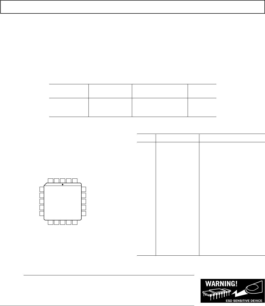
PIN DESCRIPTION
Pin No. Mnemonic Description
1 VP Positive Supply Input
2 IFN Mixer Current Output
3 AN Amplier Negative Input
4 GND Ground
5 VN Negative Supply Input
6 RFP RF Input
7 RFN RF Input
8 VN Negative Supply Input
9 VP Positive Supply Input
10 LON Local Oscillator Input
11 LOP Local Oscillator Input
12 VP Positive Supply Input
13 GND Ground
14 BIAS Bias Input
15 VN Negative Supply Input
16 OUT Amplier Output
17 VFB Amplier Feedback Input
18 COM Amplier Output Common
19 AP Amplier Positive Input
20 IFP Mixer Current Output
ABSOLUTE MAXIMUM RATINGS
1
Supply Voltage ±V
S
. . . . . . . . . . . . . . . . . . . . . . . . . . . . . ±5.5 V
Input Voltages
RFHI, RFLO . . . . . . . . . . . . . . . . . . . . . . . . . . . . . . . . .±3 V
LOHI, LOLO . . . . . . . . . . . . . . . . . . . . . . . . . . . . . . . . . ±1 V
Internal Power Dissipation
2
. . . . . . . . . . . . . . . . . . . . 1200 mW
Operating Temperature Range
AD831A . . . . . . . . . . . . . . . . . . . . . . . . . . . . –40°C to +85°C
Storage Temperature Range . . . . . . . . . . . . . . –65°C to +150°C
Lead Temperature Range (Soldering 60 sec) . . . . . . . . . . 300°C
PIN CONFIGURATION
20-Lead PLCC
CAUTION
ESD (electrostatic discharge) sensitive device. Electrostatic charges as high as 4000 V readily accumulate
on the human body and test equipment and can discharge without detection. Although the AD831 features
proprietary ESD protection circuitry, permanent damage may occur on devices subjected to high energy
electrostatic discharges. Therefore, proper ESD precautions are recommended to avoid performance
degradation or loss of functionality.
ORDERING GUIDE
Temperature Package Package
Model Range Description Option
AD831AP –40°C to +85°C 20-Lead PLCC P-20A
AD831AP-REEL7 –40°C to +85°C 20-Lead PLCC P-20A
AD831AP-EB Evaluation Board
NOTES
1
Stresses above those listed under Absolute Maximum Ratings may cause permanent
damage to the device. This is a stress rating only and functional operation of the
device at these or any other conditions above those indicated in the operational
section of this specication is not implied. Exposure to absolute maximum rating
conditions for extended periods may affect device reliability.
2
Thermal Characteristics:
20-Lead PLCC Package:
JA
= 110°C/W;
JC
= 20°C/W.
Note that the
JA
= 110°C/W value is for the package measured while suspended
in still air; mounted on a PC board, the typical value is
JA
= 90°C/W due to the
conduction provided by the AD831’s package being in contact with the board, which
serves as a heat sink.
REV. C REV. C

