AD831
–9–
For gains other than unity, the amplier’s output at OUT is
connected via an attenuator network to VFB; this determines
the overall gain. Using resistors R1 and R2 (Figure 6), the gain
setting expression is
G
R R
R
dB
=
+
Ê
Ë
Á
ˆ
¯
˜
20
1 2
2
10
log
(2)
� �
Figure 6. Output Amplier Feedback Connections
for Increasing Gain
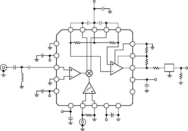
Driving Filters
The output amplier can be used for driving reverse-terminated
loads. When driving an IF band-pass lter (BPF), for example,
proper attention must be paid to providing the optimal source
and load terminations so as to achieve the specied lter response.
The AD831’s wideband highly linear output amplier affords an
opportunity to increase the RF to IF gain to compensate for a
lter’s insertion and termination losses.
Figure 7 indicates how the output amplier’s low impedance
(voltage source) output can drive a doubly terminated band-pass
lter. The typical 10 dB of loss (4 dB of insertion loss and 6 dB
due to the reverse-termination) be made up by the inclusion of a
feedback network that increases the gain of the amplier by
10 dB (3.162). When constructing a feedback circuit, the signal
path between OUT and VFB should be as short as possible.
� �
�
�
Figure 7. Connections for Driving a Doubly Terminated
Band-Pass Filter
Higher gains can be achieved, using different resistor ratios, but
with concomitant reduction in the bandwidth of this amplier
(Figure 8). Note also that the Johnson noise of these gain setting
resistors, as well as that of the BPF terminating resistors, is ulti-
mately reected back to the mixer’s input; thus they should be as
small as possible, consistent with the permissible loading on the
amplier’s output.
FREQUENCY (MHz)
12
10
0
10 1000100
1dB COMPRESSION POINT (dBm)
8
6
4
2
G = 1
G =
2
G = 4
Figure 8. Output Amplier 1 dB Compression
Point for Gains of 1, 2, and 4 (Gains of 0 dB, 6 dB,
and 12 dB, Respectively)
REV. C