AD831
–6–
AD831
–7–



        








TPC 13. Input Third Order Intercept, 9 V Single Supply



        
















TPC 14. Input Second Order Intercept, 9 V Single Supply
1200
1000
0
50 250100 150 200
800
600
400
200
4.0
3.5
3.0
2.5
2.0
INPUT CAPACITANCE
INPUT RESISTANCE
INPUT CAPACITANCE
FREQUENCY (MHz)
INPUT RESISTANCE ()
TPC 15. Input Impedance vs. Frequency, Z
IN
= R C
FREQUENCY (MHz)
18
NOISE FIGURE (dB)
16
8
50 250100 150 200
15
13
11
9
17
14
12
10
TPC 16. Noise Figure vs. Frequency,
Matched Input
REV. C
REV. C
AD831
–6–
AD831
–7–
THEORY OF OPERATION
The AD831 consists of a mixer core, a limiting amplier, a low
noise output amplier, and a bias circuit (Figure 1).
The mixer’s RF input is converted into differential currents by
a highly linear, Class A voltage-to-current converter, formed by
transistors Q1, Q2 and resistors R1, R2. The resulting currents
drive the differential pairs Q3, Q4 and Q5, Q6. The LO input is
through a high gain, low noise limiting amplier that converts the
–10 dBm LO input into a square wave. This square wave drives
the differential pairs Q3, Q4 and Q5, Q6 and produces a high
level output at IFP and IFN—consisting of the sum and differ-
ence frequencies of the RF and LO inputs—and a series of lower
level outputs caused by odd harmonics of the LO frequency mix-
ing with the RF input.
An on-chip network supplies the bias current to the RF and LO
inputs when these are ac-coupled; this network is disabled when
the AD831 is dc-coupled.
When the integral output amplier is used, pins IFN and IFP
are connected directly to pins AFN and AFP; the on-chip load
resistors convert the output current into a voltage that drives
the output amplier. The ratio of these load resistors to resistors
R1, R2 provides nominal unity gain (0 dB) from RF-to-IF. The
expression for the gain, in decibels, is
G
dB
=
Ê
Ë
Á
ˆ
¯
˜
Ê
Ë
Á
ˆ
¯
˜
Ê
Ë
Á
ˆ
¯
˜
20
4 1
2 2
10
log
p
p
(1)
where:
4
p
is the amplitude of the fundamental component of a
squarewave.
1
2
is the conversion loss.
p
2
is the small signal dc gain of the AD831 when the LO input
is driven fully positive or negative.














































 
















Figure 1. Simplied Schematic Diagram
REV. C
REV. C
AD831
–8–
AD831
–9–
Low-Pass Filtering
A simple low-pass lter may be added between the mixer and
the output amplier by shunting the internal resistive loads
(an equivalent resistance of about 14 with a tolerance of 20%)
with external capacitors; these attenuate the sum component in
a downconversion application (Figure 4). The corner frequency
of this one-pole low-pass lter (f = (2 RC
F
)
–1
) should be placed
about an octave above the difference frequency IF. Thus, for a
70 MHz IF, a –3 dB frequency of 140 MHz might be chosen,
using C
F
= (2 14 140 MHz)
–1
82 pF, the nearest
standard value.
   












 



















Figure 4. Low-Pass Filtering Using External Capacitors
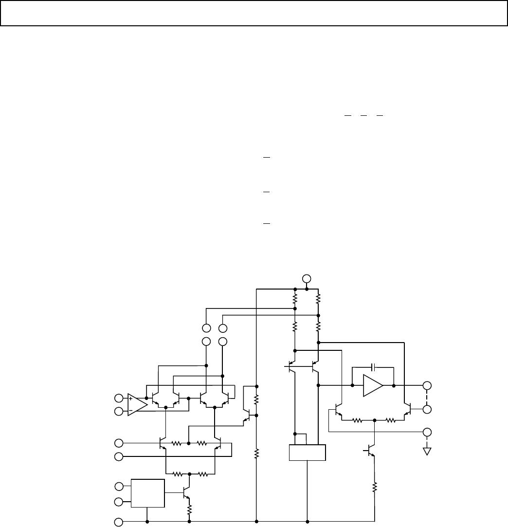
Using the Output Amplier
The AD831s output amplier converts the mixer core’s differential
current output into a single-ended voltage and provides an output
as high as ±1 V peak into a 50 V load (+10 dBm). For unity gain
operation (Figure 5), the inputs AN and AP connect to the open-
collector outputs of the mixer’s core and OUT connects to VFB.


   














 













 
Figure 5. Output Amplier Connected for Unity
Gain Operation
The mixer has two open-collector outputs (differential currents) at
pins IFN and IFP. These currents may be used to provide nominal
unity RF to IF gain by connecting a center-tapped transformer
(1:1 turns ratio) to pins IFN and IFP as shown in Figure 2.














































Figure 2. Connections for Transformer Coupling to
the IF Output
Programming the Bias Current
Because the AD831’s RF port is a Class-A circuit, the maximum
RF input is proportional to the bias current. This bias current
may be reduced by connecting a resistor from the BIAS pin to the
positive supply (Figure 3). For normal operation, the BIAS pin is
left unconnected. For lowest power consumption, the BIAS pin is
connected directly to the positive supply. The range of adjustment
is 100 mA for normal operation to 45 mA total current at minimum
power consumption.





   































Figure 3. Programming the Quiescent Current
REV. C
REV. C

AD831APZ

Mfr. #:
Manufacturer:
Analog Devices Inc.
Description:
RF Mixer Hi-Perf Low Distort 500 MHz
Lifecycle:
New from this manufacturer.
Delivery:
DHL FedEx Ups TNT EMS
Payment:
T/T Paypal Visa MoneyGram Western Union