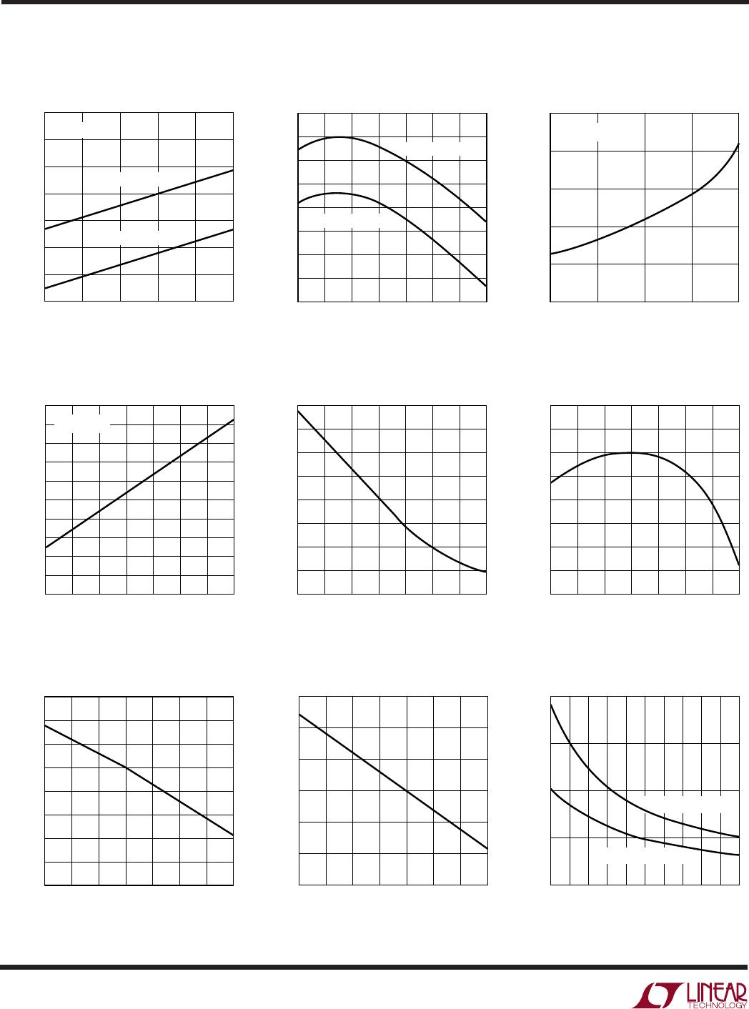
5
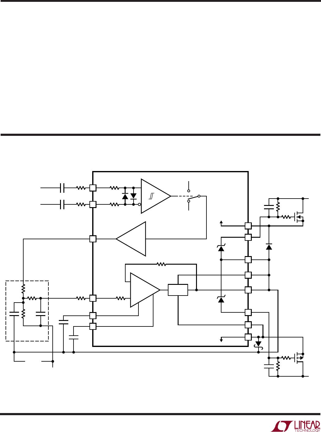
LT1684
IN B (Pin 1): PWM Negative Input. Input is isolated from
digital source by ~100pF series capacitor. A 10k resistor
can be connected to the IN B pin in series with the isolation
capacitor for transient protection. The PWM receiver imple-
ments a diode forward drop of input hysteresis (relative to
IN A). This hysteresis and internal signal limiting assure
common mode glitch rejection with isolation capacitor
mismatches up to 2:1. For maximum performance, how-
ever, effort should be made to match the two PWM input
isolation capacitors. Pin IN B is differentially clamped to
pin IN A through back-to-back diodes. This results in a
high impedance differential input through ±100mV be-
yond the input thresholds. 5k internal input resistors yield
a 10k (nominal) differential overdrive impedance.
COMP1 (Pin 2): Output Amplifier Primary Compensation.
Connect a 100pF capacitor from pin COMP1 to pin OUT.
COMP2 (Pin 3): Output Amplifier Secondary Compensa-
tion. Connect a 20pF capacitor from pin COMP2 to pin
OUT.
LIM
–
(Pin 4): Output Amplifier Current Sink Limit. Pin
implements I
OUT
• R = V
BE
current clamp. Internal clamp
resistor has a typical value of 3.5Ω. For maximum current
drive capability (190mA typical) short pin to pin V
–
.
Reduction of current sink capability is achieved by placing
additional resistance from pin LIM
–
to pin V
–
. (i.e. An
external 3.5Ω resistance from pin LIM
–
to pin V
–
will
reduce the current sinking capability of the output ampli-
fier by approximately 50%.)
V
–
(Pin 5): Local Negative Supply. Typically connected to
the source of the active tracking supply P-channel MOSFET.
V
–
rail voltage is GATE
–
self-bias voltage less the MOSFET
V
GS
. Typical P-channel MOSFET characteristics provide
AT
REF
– V
–
≈ 10V.
GATE
–
(Pin 6): Negative Power Supply FET Gate Drive. Pin
sources current from pull-down resistor to bias gate of
active tracking supply P-channel MOSFET. Self-biases to
a typical value of –14V, referenced to pin AT
REF
. Pull-down
resistor value is determined such that current sourced
from the GATE
–
pin remains greater than 50µA at mini-
mum output signal voltage and less than 10mA at maxi-
mum output signal voltage.
AT
REF
(Pin 7): Active Tracking Supply Reference. Typi-
cally connected to pin OUT. Pin bias current is the differ-
ence between the magnitudes of GATE
+
pin bias and
GATE
–
pin bias (I
ATREF
= I
GATE
+ – I
GATE
–).
OUT (Pin 8): Ring Tone Output Pin. Output of active filter
amplifier/buffer. Used as reference voltage for internal
functions of IC. Usually shorted to pin AT
REF
to generate
reference for active tracking supply circuitry. Connect a 1A
(1N4001-type) diode between V
+
and OUT and a
1A Schottky diode from V
–
to OUT for line transient
protection.
LIM
+
(Pin 9): Output Amplifier Current Source Limit. Pin
implements I
OUT
• R = V
BE
current clamp. Internal clamp
resistor has a typical value of 3.5Ω. For maximum current
drive capability (190mA typical) short pin LIM
+
to pin
OUT. Reduction of current source capability is achieved by
placing additional resistance from pin LIM
+
to pin OUT.
(i.e. An external 3.5Ω resistance from pin LIM
+
to pin OUT
will reduce the current sourcing capability of the output
amplifier by approximately 50%.)
V
+
(Pin 10): Local Positive Supply. Typically connected to
the source of the active tracking supply N-channel MOSFET.
This condition should be made using a ferrite bead.
Operating V
+
rail voltage is GATE
+
self-bias voltage less
the MOSFET V
GS
. Typical N-channel MOSFET characteris-
tics provide V
+
– AT
REF
≈ 10V.
GATE
+
(Pin 11): Positive Power Supply FET Gate Drive.
Pin sinks current from pull-up resistor to bias gate of
active tracking supply N-channel MOSFET. Self-biases to
a typical value of 14V, referenced to pin AT
REF
. Pull-up
resistor value is determined such that sink current into
GATE
+
pin remains greater than 50µA at maximum output
signal voltage and less than 10mA at minimum output
signal voltage.
AMPIN (Pin 12): Output Amplifier Input. Connected to
external filter components through series protection re-
sistor (usually 5k). Thevenin DC resistance of external
filter and protection components should be 10k for opti-
mum amplifier offset performance. See Applications In-
formation section.
UU
U
PI FU CTIO S