LC75836W
www.onsemi.com
10
Serial Data Transfer Example
• When 109 or more segments are used
All 192 bits of serial data must be sent.
• When fewer than 109 segments are used
Either 48, 96, or 144 bits of serial data must be sent, depending on the number of segments to be used. However,
the serial data shown below (the D1 to D36 display data and the control data) must always be sent.
48 bit 8 bit
D2
D
1
D23
D73
0 1 1 0 0 0 1 0
B0
B1
B2
B3
A0
A1
A2
A3
D24
D25
D26
D27
FC0
0
P0
P1
P2
FC1
FC2
OC
SC
BU
0 0
0 1 1 0 0 0 1 0
B0
B1
B2
B3
A0
A1
A2
A3
D37
0 1 1 0 0 0 1 0
B0
B1
B2
B3
A0
A1
A2
A3
D74
D38
D59
D60
D61
D62
D95
D96
0 0 0 0 0 0 0 0 0 0 0
1
0 0 0 0 0 0 0 0 0 0 0 1
D31
D63
D64
D109
0 1 1 0 0 0 1 0
B0
B1
B2
B3
A0
A1
A2
A3
D110
D131
D136
0 0 0 0 0 0 0 0 0 0 0 0 0 0 1 1
D97
D98
D99
D100
D140
D139
D138
D137
D135
D134
D133
D132
D36
D30
D29
D28
D68
D67
D66
D65
D104
D103
D102
D101
D32
D35
D34
D33
D72
D71
D70
D69
D108
D107
D106
D105
48 bit 8 bit
D2
D1
D23
0 1 1 0 0 0 1 0
B0
B1
B2
B3
A0
A1
A2
A3
D24
D25
D26
D27
FC0
0
P0
P1
P2
FC1
FC2
OC
SC
BU
0 0
D28
D32
D31
D30
D29
D36
D35
D34
D33
LC75836W
www.onsemi.com
11
Control Data Functions
1. FC0 to FC2: Common/segment output waveform frame frequency control data
These control data bits set the frame frequency of the common and segment output waveforms.
Control data
Frame frequency fo [Hz]
FC0 FC1 FC2
1 1 0
fosc/768,f
CK
/768
1 1 1
fosc/576,f
CK
/576
0 0 0
fosc/384,f
CK
/384
0 0 1
fosc/288,f
CK
/288
0 1 0
fosc/192,f
CK
/192
2. P0 to P2: Segment output port/general-purpose output port switching control data
These control data bits switch the segment output port/general-purpose output port functions of the S1/P1 to S4/P4
output pins.
Control data Output pin state
P0 P1 P2 S1/P1 S2/P2 S3/P3 S4/P4
0 0 0 S1 S2 S3 S4
0 0 1 P1 S2 S3 S4
0 1 0 P1 P2 S3 S4
0 1 1 P1 P2 P3 S4
1 0 0 P1 P2 P3 P4
Note: Sn (n = 1 to 4): Segment output ports
Pn (n = 1 to 4): General-purpose output ports
Note that when the general-purpose output port function is selected, the correspondence between the output pins and
the display data will be that shown in the table.
Output pin Corresponding display data
S1/P1 D1
S2/P2 D5
S3/P3 D9
S4/P4 D13
For example, if the general-purpose output port function is selected for the S4/P4 output pin, that output pin will
output a high level (V
DD
) when the display data D13 is 1, and a low level (V
SS
) when the D13 is 0.
3. OC: RC oscillator operating mode/external clock operating mode switching control data.
This control data bit switches the OSC pin function
(either RC oscillator operating mode or external clock operating mode).
OC OSC pin function
0 RC oscillator operating mode
1 External clock operating mode
Note: An external resistor, Rosc, and an external capacitor, Cosc, must be connected to the OSC pin if RC oscillator
operating mode is selected.
4. SC: Segment on/off control data
This control data bit controls the on/off state of the segments.
SC Display state
0 On
1 Off
Note that when the segments are turned off by setting SC to 1, the segments are turned off by outputting segment off
waveforms from the segment output pins.
5. BU: Normal mode/power-saving mode control data
This control data bit selects either normal mode or power saving mode.
BU Mode
0 Normal mode
1
Power saving mode.
In RC oscillator operating mode (OC = 0), the OSC pin oscillator is stopped, and in external clock operating mode
(OC = 1), acceptance of the external clock is stopped. In this mode the common and segment output pins go to the
V
SS
levels. However, S1/P1 to S4/P4 output pins that are set to be general-purpose output ports by the control data
P0 to P2 can be used as general-purpose output ports.
LC75836W
www.onsemi.com
12
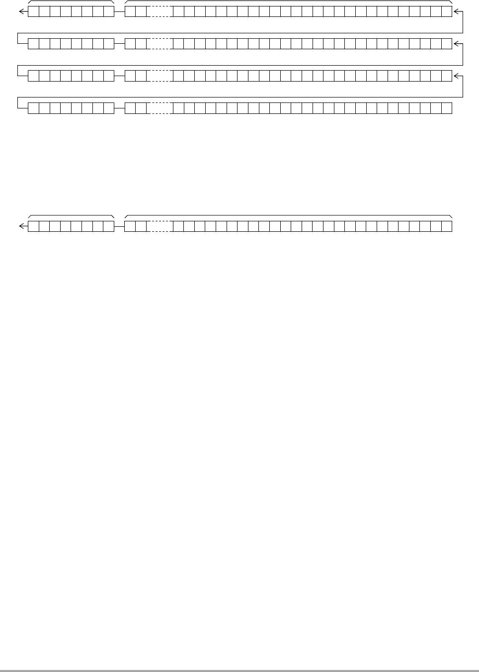
Display Data and Output Pin Correspondence
Output pin COM1 COM2 COM3 COM4
S1/P1 D1 D2 D3 D4 S19 D73 D74 D75 D76
S2/P2 D5 D6 D7 D8 S20 D77 D78 D79 D80
S3/P3 D9 D10 D11 D12 S21 D81 D82 D83 D84
S4/P4 D13 D14 D15 D16 S22 D85 D86 D87 D88
S5 D17 D18 D19 D20 S23 D89 D90 D91 D92
S6 D21 D22 D23 D24 S24 D93 D94 D95 D96
S7 D25 D26 D27 D28 S25 D97 D98 D99 D100
S8 D29 D30 D31 D32 S26 D101 D102 D103 D104
S9 D33 D34 D35 D36 S27 D105 D106 D107 D108
S10 D37 D38 D39 D40 S28 D109 D110 D111 D112
S11 D41 D42 D43 D44 S29 D113 D114 D115 D116
S12 D45 D46 D47 D48 S30 D117 D118 D119 D120
S13 D49 D50 D51 D52 S31 D121 D122 D123 D124
S14 D53 D54 D55 D56 S32 D125 D126 D127 D128
S15 D57 D58 D59 D60 S33 D129 D130 D131 D132
S16 D61 D62 D63 D64 S34 D133 D134 D135 D136
S17 D65 D66 D67 D68 S35 D137 D138 D139 D140
S18 D69 D70 D71 D72
Note: Applies when the S1/P1 to S4/P4 output pins are set to their segment output function.
For example, the table below lists the output states for the S21 output pin.
Display data
Output pin (S21) state
D81 D82 D83 D84
0 0 0 0 The LCD segments corresponding to COM1, COM2, COM3, and COM4 are off.
0 0 0 1 The LCD segment corresponding to COM4 is on.
0 0 1 0 The LCD segment corresponding to COM3 is on.
0 0 1 1 The LCD segments corresponding to COM3 and COM4 are on.
0 1 0 0 The LCD segment corresponding to COM2 is on.
0 1 0 1 The LCD segments corresponding to COM2 and COM4 are on.
0 1 1 0 The LCD segments corresponding to COM2 and COM3 are on.
0 1 1 1 The LCD segments corresponding to COM2, COM3, and COM4 are on.
1 0 0 0 The LCD segment corresponding to COM1 is on.
1 0 0 1 The LCD segments corresponding to COM1 and COM4 are on.
1 0 1 0 The LCD segments corresponding to COM1 and COM3 are on.
1 0 1 1 The LCD segments corresponding to COM1, COM3, and COM4 are on.
1 1 0 0 The LCD segments corresponding to COM1 and COM2 are on.
1 1 0 1 The LCD segments corresponding to COM1, COM2, and COM4 are on.
1 1 1 0 The LCD segments corresponding to COM1, COM2, and COM3 are on.
1 1 1 1 The LCD segments corresponding to COM1, COM2, COM3, and COM4 are on.

LC75836WH-E

Mfr. #:
Manufacturer:
ON Semiconductor
Description:
LCD Drivers LCD DISPLAY DVR
Lifecycle:
New from this manufacturer.
Delivery:
DHL FedEx Ups TNT EMS
Payment:
T/T Paypal Visa MoneyGram Western Union

Products related to this Datasheet