LT5528
1
5528f
The LT
®
5528 is a direct I/Q modulator designed for high
performance wireless applications, including wireless
infrastructure. It allows direct modulation of an RF signal
using differential baseband I and Q signals. It supports
PHS, GSM, EDGE, TD-SCDMA, CDMA, CDMA2000,
W-CDMA and other systems. It may also be confi gured
as an image reject up-converting mixer, by applying
90° phase-shifted signals to the I and Q inputs. The I/Q
baseband inputs consist of voltage-to-current converters
that in turn drive double-balanced mixers. The outputs of
these mixers are summed and applied to an on-chip RF
transformer, which converts the differential mixer signals
to a 50Ω single-ended output. The four balanced I and Q
baseband input ports are intended for DC coupling from a
source with a common-mode voltage level of about 0.5V.
The LO path consists of an LO buffer with single-ended
input, and precision quadrature generators that produce
the LO drive for the mixers. The supply voltage range is
4.5V to 5.25V.
Direct Conversion to 1.5GHz to 2.4GHz
High OIP3: 21.8dBm at 2GHz
Low Output Noise Floor at 5MHz Offset:
No RF: –159.3dBm/Hz
P
OUT
= 4dBm: –151.8dBm/Hz
4-Ch W-CDMA ACPR: –66dBc at 2.14GHz
Integrated LO Buffer and LO Quadrature Phase
Generator
50Ω AC-Coupled Single-Ended LO and RF Ports
50Ω DC Interface to Baseband Inputs
Low Carrier Leakage: –42dBm at 2GHz
High Image Rejection: 45dB at 2GHz
16-Lead QFN 4mm × 4mm Package
1.5GHz to 2.4GHz Direct Conversion Transmitter Application
with LO Feed-Through and Image Calibration Loop
90°
LT5528
BASEBAND
DSP
CAL
LO FEED-THROUGH CAL OUT
IMAGE CAL OUT
PA
VCO/SYNTHESIZER
RF = 1.5GHz
TO 2.4GHz
EN
2, 4, 6, 9, 10, 12, 15, 17
5V
V-I
V-I
I-CHANNEL
Q-CHANNEL
BALUN
14
16
1
7
5
8, 13
V
CC
11
3
5528 TA01a
I-DAC
Q-DAC
ADC
1.5GHz to 2.4GHz
High Linearity Direct
Quadrature Modulator
Infrastructure Tx for DCS, PCS and UMTS Bands
Image Reject Up-Converters for PCS and UMTS
Bands
Low-Noise Variable Phase-Shifter for 1.5GHz to
2.4GHz Local Oscillator Signals
RF OUTPUT POWER PER CARRIER (dBm)
–38–42
ACPR, AltCPR (dBc)
–55
–60
–65
–70
–75
–80
NOISE FLOOR AT 30MHz OFFSET (dBm/Hz)
–140
–150
–145
–155
–165
–160
5528 TA01b
–14–18–22–26–30–34
4-CH ACPR
2-CH ACPR
1-CH ACPR
4-CH AltCPR
2-CH AltCPR
DOWNLINK TEST MODEL 64 DPCH
1-CH AltCPR
4-CH NOISE
1-CH NOISE
W-CDMA ACPR, AltCPR and Noise vs RF Output
Power at 2140MHz for 1, 2 and 4 Channels
APPLICATIO S
U
FEATURES
DESCRIPTIO
U
TYPICAL APPLICATIO
U
, LTC and LT are registered trademarks of Linear Technology Corporation.
LT5528
2
5528f
ORDER PART
NUMBER
UF PART
MARKING
T
JMAX
= 125°C, θ
JA
= 37°C/W
EXPOSED PAD IS GROUND (PIN 17)
MUST BE SOLDERED TO PCB.
Consult LTC Marketing for parts specifi ed with wider operating temperature ranges.
5528A
LT5528EUF
(Note 1)
Supply Voltage .........................................................5.5V
Common-Mode Level of BBPI, BBMI and
BBPQ, BBMQ .......................................................2.5V
Operating Ambient Temperature
(Note 2) ...............................................40°C to 85°C
Storage Temperature Range ..................65°C to 125°C
Voltage on Any Pin
Not to Exceed ......................500mV to V
CC
+ 500mV
V
CC
= 5V, EN = High, T
A
= 25°C, f
LO
= 2GHz, f
RF
= 2.002GHz, P
LO
= 0dBm.
BBPI, BBMI, BBPQ, BBMQ inputs 0.525V
DC
, Baseband Input Frequency = 2MHz, I&Q 90° shifted (upper sideband selection).
P
RF, OUT
= –10dBm, unless otherwise noted. (Note 3)
SYMBOL PARAMETER CONDITIONS MIN TYP MAX UNITS
RF Output (RF)
f
RF
RF Frequency Range 3dB Bandwidth 1.5 to 2.4 GHz
RF Frequency Range 1dB Bandwidth 1.7 to 2.2 GHz
S
22, ON
RF Output Return Loss EN = High (Note 6) 15 dB
S
22, OFF
RF Output Return Loss EN = Low (Note 6) 12 dB
NFloor RF Output Noise Floor No Input Signal (Note 8) 159.3 dBm/Hz
P
OUT
= 4dBm (Note 9) 151.8 dBm/Hz
P
OUT
= 4dBm (Note 10) 151.8 dBm/Hz
G
P
Conversion Power Gain P
OUT
/P
IN, I&Q
6.5 dB
G
V
Conversion Voltage Gain 20 • Log (V
OUT, 50Ω
/V
IN, DIFF, I or Q
) 6 dB
P
OUT
Absolute Output Power 1V
P-P DIFF
CW Signal, I and Q 2.1 dBm
G
3LO vs LO
3 • LO Conversion Gain Difference (Note 17) 28 dB
OP1dB Output 1dB Compression (Note 7) 7.9 dBm
OIP2 Output 2nd Order Intercept (Notes 13, 14) 49 dBm
OIP3 Output 3rd Order Intercept (Notes 13, 15) 21.8 dBm
IR Image Rejection (Note 16) 45 dBc
LOFT Carrier Leakage EN = High, P
LO
= 0dBm (Note 16) 42 dBm
(LO Feed-Through) EN = Low, P
LO
= 0dBm (Note 16) 57.8 dBm
LO Input (LO)
f
LO
LO Frequency Range 1.5 to 2.4 GHz
P
LO
LO Input Power 10 0 5 dBm
S
11, ON
LO Input Return Loss EN = High (Note 6) 17 dB
S
11, OFF
LO Input Return Loss EN = Low (Note 6) 5.5 dB
NF
LO
LO Input Referred Noise Figure (Note 5) at 2GHz 14.4 dB
G
LO
LO to RF Small Signal Gain (Note 5) at 2GHz 20.4 dB
IIP3
LO
LO Input 3rd Order Intercept (Note 5) at 2GHz 10 dBm
ELECTRICAL CHARACTERISTICS
ABSOLUTE AXI U RATI GS
W
WW
U
PACKAGE/ORDER I FOR ATIO
UUW
16 15 14 13
5 6 7 8
TOP VIEW
9
10
11
12
4
3
2
1EN
GND
LO
GND
GND
RF
GND
GND
BBMI
GND
BBPI
V
CC
BBMQ
GND
BBPQ
V
CC
17
UF PACKAGE
16-LEAD (4mm × 4mm) PLASTIC QFN
LT5528
3
5528f
V
CC
= 5V, EN = High, T
A
= 25°C, f
LO
= 2GHz, f
RF
= 2.002GHz, P
LO
= 0dBm.
BBPI, BBMI, BBPQ, BBMQ inputs 0.525V
DC
, Baseband Input Frequency = 2MHz, I&Q 90° shifted (upper sideband selection).
P
RF, OUT
= –10dBm, unless otherwise noted. (Note 3)
Note 1: Absolute Maximum Ratings are those values beyond which the life
of a device may be impaired.
Note 2: Specifi cations over the –40°C to 85°C temperature range are
assured by design, characterization and correlation with statistical process
controls.
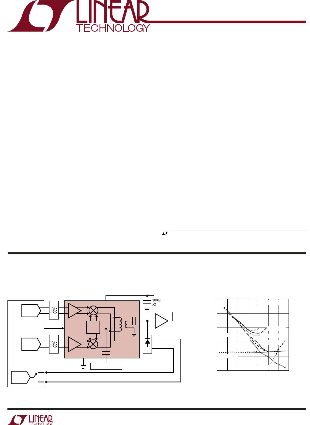
Note 3: Tests are performed as shown in the confi guration of Figure 7.
Note 4: On each of the four baseband inputs BBPI, BBMI, BBPQ and
BBMQ.
Note 5: V(BBPI) – V(BBMI) = 1V
DC
, V(BBPQ) – V(BBMQ) = 1V
DC
.
Note 6: Maximum value within –1dB bandwidth.
Note 7: An external coupling capacitor is used in the RF output line.
Note 8: At 20MHz offset from the LO signal frequency.
Note 9: At 20MHz offset from the CW signal frequency.
Note 10: At 5MHz offset from the CW signal frequency.
Note 11: RF power is within 10% of fi nal value.
Note 12: RF power is at least 30dB lower than in the ON state.
Note 13: Baseband is driven by 2MHz and 2.1MHz tones. Drive level is set
in such a way that the two resulting RF tones are –10dBm each.
Note 14: IM2 measured at LO frequency + 4.1MHz.
Note 15: IM3 measured at LO frequency + 1.9MHz and LO frequency +
2.2MHz.
Note 16: Amplitude average of the characterization data set without image
or LO feed-through nulling (unadjusted).
Note 17: The difference in conversion gain between the spurious signal at
f = 3 • LO – BB versus the conversion gain at the desired signal at f = LO +
BB for BB = 2MHz and LO = 2GHz.
SYMBOL PARAMETER CONDITIONS MIN TYP MAX UNITS
Baseband Inputs (BBPI, BBMI, BBPQ, BBMQ)
BW
BB
Baseband Bandwidth 3dB Bandwidth 400 MHz
V
CMBB
DC Common Mode Voltage (Note 4) 0.525 V
R
IN, SE
Single-Ended Input Resistance (Note 4) 45 Ω
P
LO2BB
Carrier Feed-Through on BB P
OUT
= 0 (Note 4) 40 dBm
IP1dB Input 1dB Compression Point Differential Peak-to-Peak (Note 7) 3.2 V
P-P, DIFF
ΔG
I/Q
I/Q Absolute Gain Imbalance 0.05 dB
Δϕ
I/Q
I/Q Absolute Phase Imbalance 0.5 Deg
Power Supply (V
CC
)
V
CC
Supply Voltage 4.5 5 5.25 V
I
CC, ON
Supply Current EN = High 125 145 mA
I
CC, OFF
Supply Current, Sleep Mode EN = 0V 0.05 50 µA
t
ON
Turn-On Time EN = Low to High (Note 11) 0.25 µs
t
OFF
Turn-Off Time EN = High to Low (Note 12) 1.3 µs
Enable (EN), Low = Off, High = On
Enable Input High Voltage EN = High 1.0 V
Input High Current EN = 5V 240 µA
Sleep Input Low Voltage EN = Low 0.5 V
ELECTRICAL CHARACTERISTICS

LT5528EUF#PBF

Mfr. #:
Manufacturer:
Analog Devices Inc.
Description:
Modulator / Demodulator 2GHz Direct Quadrature Modulator
Lifecycle:
New from this manufacturer.
Delivery:
DHL FedEx Ups TNT EMS
Payment:
T/T Paypal Visa MoneyGram Western Union

Products related to this Datasheet