LT5528
13
5528f
Application Measurements
The LT5528 is recommended for base-station applications
using various modulation formats. Figure 12 shows a typi-
cal application. The CAL box in Figure 12 allows for LO
feed-through and Image suppression calibration.
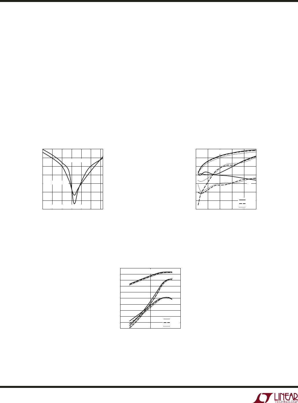
Figure 13 shows the ACPR performance for W-CDMA using
one, two or four channel modulation. Figures 14, 15 and 16
illustrate the 1-, 2- and 4-channel W-CDMA measurement.
To calculate ACPR, a correction is made for the spectrum
analyzer noise fl oor. If the output power is high, the ACPR
will be limited by the linearity performance of the part. If
the output power is low, the ACPR will be limited by the
noise performance of the part. In the middle, an optimum
ACPR is obtained.
Because of the LT5528’s very high dynamic-range, the
test equipment can limit the accuracy of the ACPR mea-
surement. Consult the factory for advice on the ACPR
measurement, if needed.
The ACPR performance is sensitive to the amplitude match
of the BBIP and BBIM (or BBQP and BBQM) inputs. This
is because a difference in AC current amplitude will give
rise to a difference in amplitude between the even-order
harmonic products generated in the internal V-I converter.
As a result, they will not cancel out entirely. Therefore, it
is important to keep the currents in those pins exactly the
same (but of opposite sign). The current will enter the
LT5528’s common-base stage, and will fl ow to the mixer
upper switches. This can be seen in Figure 1 where the
Figure 12. 1.5GHz to 2.4GHz Direct Conversion Transmitter Application with
LO Feed-Through and Image Calibration Loop
90°
LT5528
BASEBAND
GENERATOR
CAL
LO FEED-THROUGH CAL OUT
IMAGE CAL OUT
PA
VCO/SYNTHESIZER
RF = 1.5GHz
TO 2.4GHz
EN
2, 4, 6, 9, 10, 12, 15, 17
5V
V-I
V-I
I-CHANNEL
Q-CHANNEL
BALUN
14
16
1
7
5
8, 13
V
CC
11
3
5528 F12
I-DAC
Q-DAC
ADC
Figure 14: 1-Channel W-CDMA Spectrum
RF FREQUENCY (MHz)
2127.5
POWER IN 30kHz BW (dBm)
5528 F14
2142.52137.52132.5 2147.5
2152.5
–30
–40
–60
–70
–80
–90
–120
–110
–100
–50
SYSTEM
NOISE FLOOR
CORRECTED
SPECTRUM
DOWNLINK TEST
MODEL 64 DPCH
UNCORRECTED
SPECTRUM
Figure 15: 2-Channel W-CDMA Spectrum
RF FREQUENCY (MHz)
2125
POWER IN 30kHz BW (dBm)
5528 F15
214021352130 2145
21552150
–30
–40
–60
–70
–80
–90
–120
–110
–100
–50
UNCOR-
RECTED
SPECTRUM
SYSTEM
NOISE FLOOR
CORRECTED
SPECTRUM
DOWNLINK TEST
MODEL 64
DPCH
Figure 13: W-CDMA APCR, AltCPR and Noise
vs RF Output Power at 2140MHz for 1, 2 and
4 Channels
RF OUTPUT POWER PER CARRIER (dBm)
–38–42
ACPR, AltCPR (dBc)
–55
–60
–65
–70
–75
–80
NOISE FLOOR AT 30MHz OFFSET (dBm/Hz)
–140
–150
–145
–155
–165
–160
5528 F13
–14–18–22–26–30–34
4-CH ACPR
2-CH ACPR
1-CH ACPR
4-CH AltCPR
2-CH AltCPR
DOWNLINK TEST MODEL 64 DPCH
1-CH AltCPR
4-CH NOISE
1-CH NOISE
Figure 16: 4-Channel W-CDMA Spectrum
DOWNLINK
TEST
MODEL 64
DPCH
RF FREQUENCY (MHz)
2115
POWER IN 30kHz BW (dBm)
5528 F16
214521352125 2155
2165
–40
–60
–70
–80
–90
–130
–120
–110
–100
–50
UNCOR-
RECTED
SPECTRUM
SYSTEM
NOISE FLOOR
CORRECTED SPECTRUM
CORRECTED
SPECTRUM
APPLICATIO S I FOR ATIO
WUU
U
LT5528
14
5528f
internal circuit of the LT5528 is drawn. For best results,
a high ohmic source is recommended; for example, the
interface circuit drawn in Figure 3, modifi ed by pulling
resistors R5 and R6 to a –5V supply and adjusting their
values to 550Ω, with T1 omitted.
Another method to reduce current mismatch between
the currents fl owing in the BBIP and BBIM pins (or the
BBQP and BBQM pins) is to use a 1:1 transformer with
the two windings in the DC path (T1 in Figure 3). For DC,
the transformer forms a short, and for AC, the transformer
will reduce the common-mode current component, which
forces the two currents to be better matched. Alternatively,
a transformer with 1:2 impedance ratio can be used, which
gives a convenient DC separation between primary and
secondary in combination with the required impedance
match. The secondary center tap should not be connected,
which allows some voltage swing if there is a single-
ended input impedance difference at the baseband pins.
As a result, both currents will be equal. The disadvantage
is that there is no DC coupling, so the LO feed-through
calibration cannot be performed via the BB connections.
After calibration when the temperature changes, the LO
feed-through and the Image Rejection performance will
change. This is illustrated in Figure 17. The LO feed-through
and Image Rejection can also change as a function of the
baseband drive level, as is depicted in Figure 18. The RF
output power, IM2 and IM3 vs a two-tone baseband drive
are given in Figure 19.
Figure 18: LO Feed-Through and Image Rejection vs Baseband
Drive Voltage after Calibration at 25°C
0
123
54
I AND Q BASEBAND VOLTAGE (V
P-P, DIFF
)
LOFT (dBm), IR (dBc)
–90
–80
–20
–30
–40
–60
–50
–70
P
RF
(dBm)
10
0
–10
–20
–30
–40
–60
–50
–40°C
25°C
85°C
5528 F18
EN = HIGH
V
CC
= 5V
f
BBI
= 2MHz, 0°
f
BBQ
= 2MHz, 90°
f
LO
= 2.14GHz
f
RF
= f
BB
+ f
LO
P
LO
= 0dBm
IR
P
RF
LOFT
Figure 17: LO Feed-Through and Image Rejection vs Temperature
after Calibration at 25°C
–40
–20 0 20
8040 60
TEMPERATURE (°C)
LOFT (dBm), IR (dB)
–85
–80
–50
–55
–60
–70
–65
–75
5528 F18
EN = HIGH
V
CC
= 5V
f
BBI
= 2MHz, 0°
f
BBQ
= 2MHz, 90°
f
LO
= 2.14GHz
f
RF
= f
BB
+ f
LO
P
LO
= 0dBm
CALIBRATED WITH P
RF
= –10dBm
LO FEED-THROUGH
IMAGE REJECTION
Figure 19: RF Two-Tone Power, IM2 and IM3 at 2140MHz vs Baseband Voltage
0.1
1
10
I AND Q BASEBAND VOLTAGE (V
P-P, DIFF
EACH TONE)
P
RF
, EACH TONE (dBm), IM2, IM3 (dBm)
–90
–80
10
0
–20
–10
–30
–40
–60
–50
–70
–40°C
25°C
85°C
5528 F19
EN = HIGH
V
CC
= 5V
f
BBI
= 2MHz, 2.1MHz, 0°
f
BBQ
= 2MHz, 2.1MHz, 90°
IM2 = POWER AT f
LO
+ 4.1MHz
IM3 = MAX POWER AT f
LO
+ 1.9MHz OR
f
LO
+ 2.2MHz
f
LO
= 2.14GHz
f
RF
= f
BB
+ f
LO
P
LO
= 0dBm
P
RF
IM2
IM3
APPLICATIO S I FOR ATIO
WUU
U
LT5528
15
5528f
Information furnished by Linear Technology Corporation is believed to be accurate and reliable.
However,
no responsibility is assumed for its use. Linear Technology Corporation makes no representation that
the interconnection of its circuits as described herein will not infringe on existing patent rights.
UF Package
16-Lead Plastic QFN (4mm × 4mm)
(Reference LTC DWG # 05-08-1692)
4.00 ± 0.10
(4 SIDES)
NOTE:
1. DRAWING CONFORMS TO JEDEC PACKAGE OUTLINE MO-220 VARIATION (WGGC)
2. DRAWING NOT TO SCALE
3. ALL DIMENSIONS ARE IN MILLIMETERS
4. DIMENSIONS OF EXPOSED PAD ON BOTTOM OF PACKAGE DO NOT INCLUDE
MOLD FLASH. MOLD FLASH, IF PRESENT, SHALL NOT EXCEED 0.15mm ON ANY SIDE
5. EXPOSED PAD SHALL BE SOLDER PLATED
6. SHADED AREA IS ONLY A REFERENCE FOR PIN 1 LOCATION
ON THE TOP AND BOTTOM OF PACKAGE
PIN 1
TOP MARK
(NOTE 6)
0.55 ± 0.20
1615
1
2
BOTTOM VIEW—EXPOSED PAD
2.15 ± 0.10
(4-SIDES)
0.75 ± 0.05
R = 0.115
TYP
0.30 ± 0.05
0.65 BSC
0.200 REF
0.00 – 0.05
(UF) QFN 1103
RECOMMENDED SOLDER PAD PITCH AND DIMENSIONS
0.72 ±0.05
0.30 ±0.05
0.65 BSC
2.15 ± 0.05
(4 SIDES)
2.90 ± 0.05
4.35 ± 0.05
PACKAGE OUTLINE
PACKAGE DESCRIPTIO
U

LT5528EUF#PBF

Mfr. #:
Manufacturer:
Analog Devices Inc.
Description:
Modulator / Demodulator 2GHz Direct Quadrature Modulator
Lifecycle:
New from this manufacturer.
Delivery:
DHL FedEx Ups TNT EMS
Payment:
T/T Paypal Visa MoneyGram Western Union

Products related to this Datasheet