LT5528
10
5528f
LO Section
The internal LO input amplifi er performs single-ended to
differential conversion of the LO input signal. Figure 4
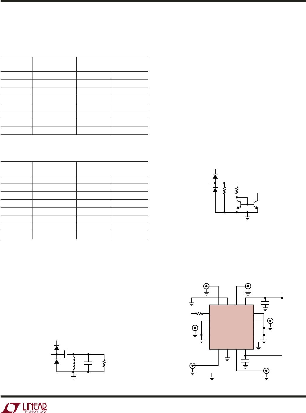
shows the equivalent circuit schematic of the LO input.
Table 1. LO Port Input Impedance vs Frequency for EN = High
Frequency Input Impedance S
11
MHz Ω Mag Angle
1000 49.9 + j18.5 0.182 80
1400 68.1 + j8.8 0.171 22
1600 71.0 + j2.0 0.175 4.8
1800 70.0 – j8.6 0.182 –6.6
2000 62.0 – j12.8 0.156 –40
2200 53.8 – j13.6 0.135 –66
2400 47.3 – j12.4 0.128 –95
2600 41.1 – j12.0 0.161 –119
If the part is in shut-down mode, the input impedance of
the LO port will be different. The LO input impedance for
EN = Low is given in Table 2.
Table 2. LO Port Input Impedance vs Frequency for EN = Low
Frequency Input Impedance S
11
MHz Ω Mag Angle
1000 46.6 + j47.6 0.443 67.8
1400 136 + j44.5 0.507 13.8
1600 157 – j24.5 0.526 –6.2
1800 114 – j70.6 0.533 –24.6
2000 70.7 – j72.1 0.533 –43.2
2200 45.3 – j59.0 0.528 –62.8
2400 31.2 – j45.2 0.527 –83.5
2600 22.8 – j34.2 0.543 –103
RF Section
After up-conversion, the RF outputs of the I and Q mixers are
combined. An on-chip balun performs internal differential
to single-ended output conversion, while transforming the
output signal impedance to 50Ω. Table 3 shows the RF
port output impedance vs. frequency.
Table 3. RF Port Output Impedance vs Frequency for EN = High
and P
LO
= 0dBm
Frequency Output Impedance S
22
MHz Ω Mag Angle
1000 23.1 + j7.9 0.382 158
1400 34.4 + j20.7 0.298 113
1600 45.8 + j22.3 0.231 87.6
1800 54.5 + j12.4 0.125 63.2
2000 48.7 + j1.7 0.022 127
2200 39.1 + j1.0 0.123 174
2400 32.9 + j4.4 0.213 163
2600 29.7 + j7.4 0.269 155
LO
INPUT
20pF
Z
IN
≈ 57Ω
5528 F04
V
CC
The internal, differential LO signal is then split into in-
phase and quadrature (90° phase shifted) signals that
drive LO buffer sections. These buffers drive the double
balanced I and Q mixers. The phase relationship between
the LO input and the internal in-phase LO and quadrature
LO signals is fi xed, and is independent of start-up condi-
tions. The phase shifters are designed to deliver accurate
quadrature signals for an LO frequency near 2GHz. For
frequencies signifi cantly below 1.8GHz or above 2.4GHz,
the quadrature accuracy will diminish, causing the image
rejection to degrade. The LO pin input impedance is about
50Ω, and the recommended LO input power is 0dBm. For
lower LO input power, the gain, OIP2, OIP3 and dynamic-
range will degrade, especially below –5dBm and at T
A
=
85°C. For high LO input power (e.g. 5dBm), the LO feed-
through will increase with no improvement in linearity or
gain. Harmonics present on the LO signal can degrade the
image rejection because they can introduce a small excess
phase shift in the internal phase splitter. For the second (at
4GHz) and third harmonics (at 6GHz) at –20dBc level, the
introduced signal at the image frequency is about –56dBc
or lower, corresponding to an excess phase shift much
below 1 degree. For the second and third harmonics at
–10dBc, the introduced signal at the image frequency is
about –47dBc. Higher harmonics than the third will have
less impact. The LO return loss typically will be better than
17dB over the 1.7GHz to 2.3GHz range. Table 1 shows the
LO port input impedance vs. frequency.
Figure 4. Equivalent Circuit Schematic of the LO Input
APPLICATIO S I FOR ATIO
WUU
U