LT5528
7
5528f
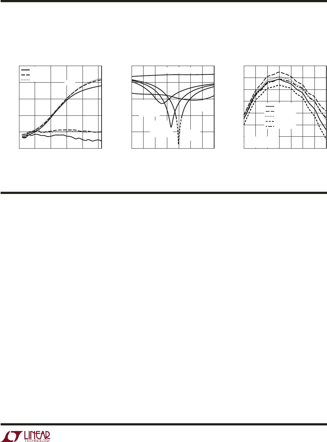
LO and RF Port Return Loss vs
RF Frequency
0
123
54
I AND Q BASEBAND VOLTAGE (V
P-P, DIFF
)
LOFT (dBm), IR (dBc)
–25
–30
–40
–45
–35
–50
5528 G18
f
BBI
= 2MHz, 0°
f
BBQ
= 2MHz, 90°
IR
LOFT
4.5V
5V
5.5V
RF FREQUENCY (GHz)
1.3
S
11
(dB)
5528 G19
1.91.71.5 2.1 2.3
2.
2.5
0
–10
–20
–30
–40
–50
RF PORT,
EN = HIGH,
P
LO
= OFF
RF PORT,
EN = LOW
LO PORT,
EN = HIGH
LO PORT, EN = LOW
RF PORT,
EN = HIGH,
P
LO
= 0dBm
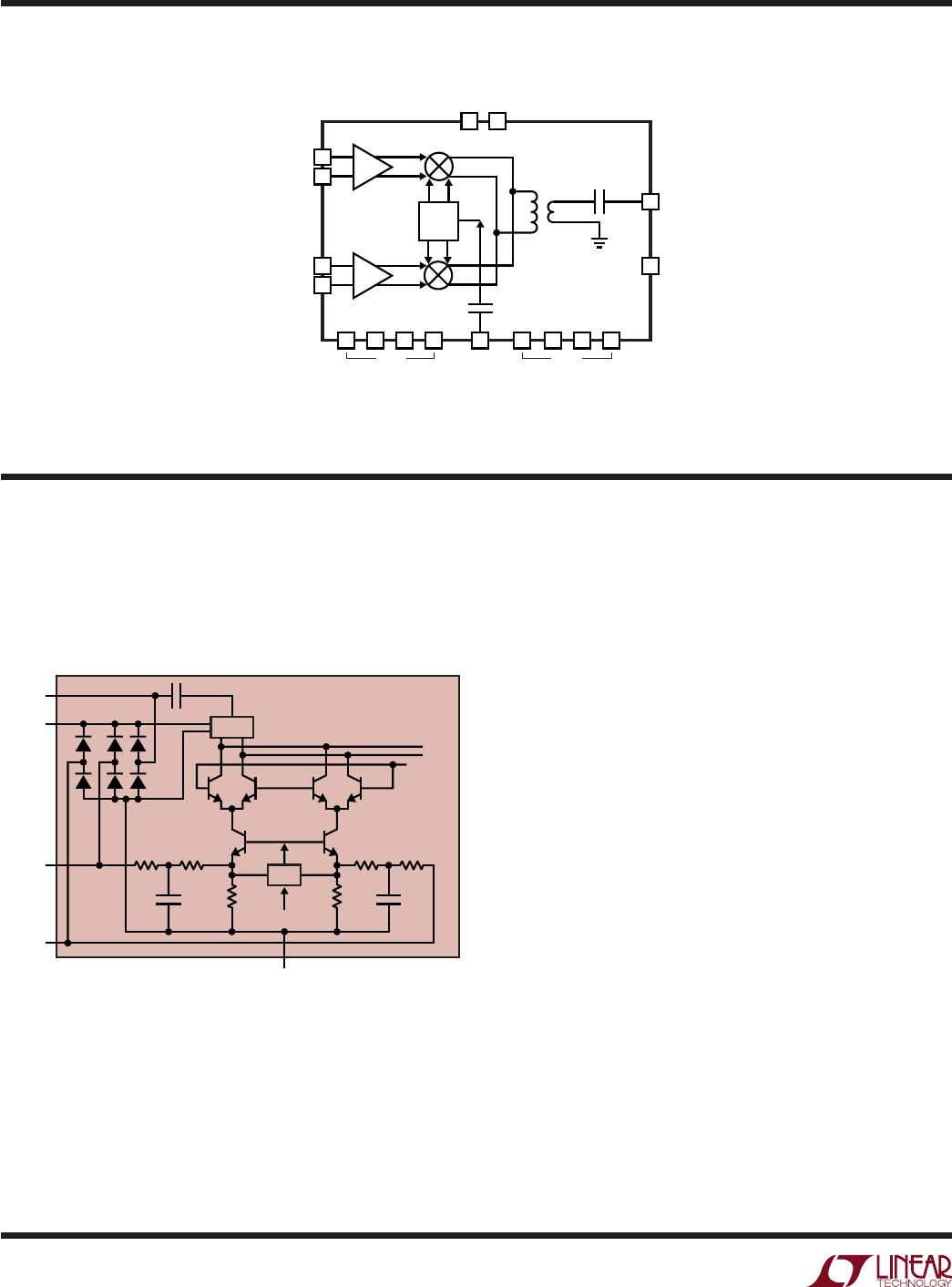
EN (Pin 1): Enable Input. When the EN pin voltage is higher
than 1V, the IC is turned on. When the input voltage is less
than 0.5V, the IC is turned off.
GND (Pins 2, 4, 6, 9, 10, 12, 15): Ground. Pins 6, 9, 15
and 17 (exposed pad) are connected to each other inter-
nally. Pins 2 and 4 are connected to each other internally
and function as the ground return for the LO signal. Pins
10 and 12 are connected to each other internally and
function as the ground return for the on-chip RF balun.
For best RF performance, pins 2, 4, 6, 9, 10, 12, 15 and
the Exposed Pad 17 should be connected to the printed
circuit board ground plane.
LO (Pin 3): LO Input. The LO input is an AC-coupled single-
ended input with approximately 50Ω input impedance at
RF frequencies. Externally applied DC voltage should be
within the range –0.5V to V
CC
+ 0.5V in order to avoid
turning on ESD protection diodes.
BBPQ, BBMQ (Pins 7, 5): Baseband Inputs for the Q-chan-
nel, each 45Ω input impedance. Internally biased at about
0.525V. Applied voltage must stay below 2.5V.
V
CC
(Pins 8, 13): Power Supply. Pins 8 and 13 are con-
nected to each other internally. It is recommended to use
0.1µF capacitors for decoupling to ground on each of
these pins.
RF (Pin 11): RF Output. The RF output is an AC-coupled
single-ended output with approximately 50Ω output im-
pedance at RF frequencies. Externally applied DC voltage
should be within the range –0.5V to V
CC
+ 0.5V in order
to avoid turning on ESD protection diodes.
BBPI, BBMI (Pins 14, 16): Baseband Inputs for the
I-channel, each with 45Ω input impedance. These pins are
internally biased at about 0.525V. Applied voltage must
stay below 2.5V.
Exposed Pad (Pin 17): Ground. This pin must be soldered
to the printed circuit board ground plane.
LO Feed-Through and Image
Rejection at 2140MHz vs Baseband
Voltage and Supply Voltage
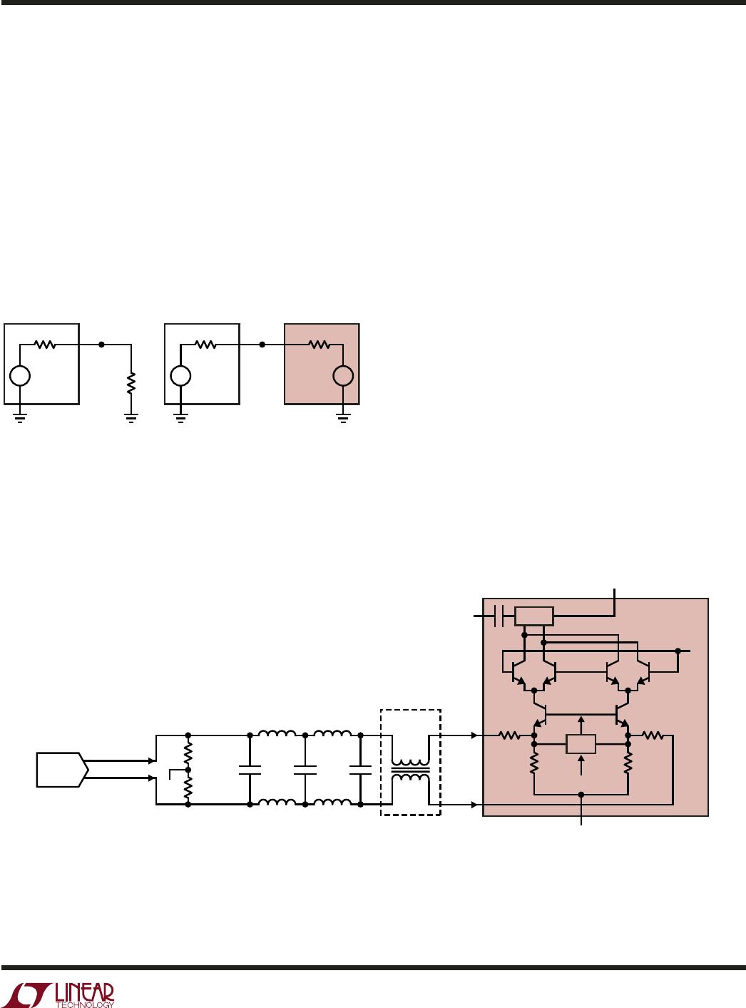
V
CC
= 5V, EN = High, T
A
= 25°C, f
LO
= 2.14GHz, P
LO
= 0dBm. BBPI, BBMI, BBPQ, BBMQ inputs 0.525V
DC
, Baseband Input Frequency f
BB
= 2MHz, I&Q 90° shifted. f
RF
= f
BB
+ f
LO
(upper
sideband selection). P
RF, OUT
= –10dBm (–10dBm/tone for 2-tone measurements), unless otherwise noted. (Note 3)
RF Output Power vs
RF Frequency at 1V
P-P
Differential Baseband Drive
RF FREQUENCY (GHz)
1.3
RF OUTPUT POWER (dBm)
0
–2
–4
–6
–8
–10
–14
–12
5528 G20
1.91.71.5 2.1 2.3
2.
2.5
4.5V, 25°C
5V, –40°C
5V, 25°C
5V, 85°C
5.5V, 25°C
V
BBI
= 1V
P-P, DIFF
V
BBQ
= 1V
P-P, DIFF
TYPICAL PERFOR A CE CHARACTERISTICS
UW
PI FU CTIO S
UUU