DATASHEET
EIGHT OUTPUT DIFFERENTIAL BUFFER FOR PCIE GEN1,2,3
9DB833
IDT®
EIGHT OUTPUT DIFFERENTIAL BUFFER FOR PCIE GEN1,2,3 1
9DB833 REV H 06/07/16
General Description
The 9DB833 zero-delay buffer supports PCIe Gen3
requirements, while being backwards compatible to PCIe
Gen2 and Gen1. The 9DB833 is driven by a differential
SRC output pair from an IDT 932S421 or 932SQ420 or
equivalent main clock generator.
Recommended Application
8 output PCIe Gen1,2,3 zero-delay/fanout buffer
Output Features
• 8 - 0.7V current-mode differential HCSL output pairs
• Supports zero delay buffer mode and fanout mode
• Selectable bandwidth
• 50-110 MHz operation in PLL mode
• 5-166 MHz operation in Bypass mode
Features/Benefits
• 3 Selectable SMBus Addresses; multiple devices can
share the same SMBus Segment
• OE# pins; suitable for Express Card applications
• PLL or bypass mode; PLL can dejitter incoming clock
• Selectable PLL bandwidth; minimizes jitter peaking in
downstream PLL's
• Spread Spectrum Compatible; tracks spreading input
clock for low EMI
• SMBus Interface; unused outputs can be disabled
• Supports undriven differential outputs in Power Down
mode for power management
Key Specifications
• Outputs cycle-cycle jitter <50ps
• Output to Output skew <50ps
• Phase jitter: PCIe Gen3 <1.0ps rm
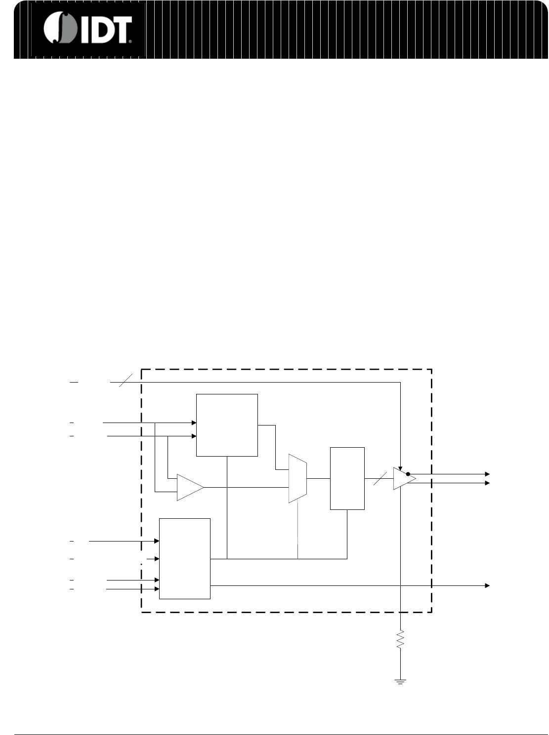
Block Diagram
LOCK
STOP
LOGIC
SRC_IN
SRC_IN#
DIF(7:0))
CONTROL
LOGIC
BYP#_LOBW_HIBW
SMBDAT
SMBCLK
PD#
SPREAD
COMPATIBLE
PLL
8
IREF
OE(7:0)#
8
M
U
X