9DB833
EIGHT OUTPUT DIFFERENTIAL BUFFER FOR PCIE GEN1,2,3
IDT®
EIGHT OUTPUT DIFFERENTIAL BUFFER FOR PCIE GEN1,2,3 4
9DB833 REV H 06/07/16
Pin Descriptions (cont.)
PIN # PI N NAME PIN TYPE DESCR IPTION
25 GND PWR Ground pin.
26 GND PWR Ground pin.
27 VDD PWR Power supply, nominal 3.3V
28 SMB_ ADR_tri IN
SMBus address select bit. This is a tri-level input that decodes 1 of 3 SMBus
Addresses.
29 DIF_4# OUT 0.7V differential Complementary clock output
30 DIF_4 OUT 0.7V differential true clock output
31 VDD PWR Power supply, nominal 3.3V
32 GND PWR Ground pin.
33 DIF_5# OUT 0.7V differential Complementary clock output
34 DIF_5 OUT 0.7V differential true clock output
35 OE5# IN
Active low input for enabling DIF pair 5.
1 =disable outputs, 0 = enable outputs
36 OE6# IN
Active low input for enabling DIF pair 6.
1 =disable outputs, 0 = enable outputs
37 DIF_6# OUT 0.7V differential Complementary clock output
38 DIF_6 OUT 0.7V differential true clock output
39 VDD PWR Power supply, nominal 3.3V
40 PD# IN
Asynchronous active low input pin used to power dow n the device. The internal
clocks are disabled and the VCO and the crystal osc. (if any) are stopped.
41 DIF_7# OUT 0.7V differential Com
p
lementar
y
clock out
p
ut
42 DIF_7 OUT 0.7V differential true clock out
p
ut
43 OE4# IN
Active low input for enabling DIF pair 4
1 =disable out
p
uts, 0 = enable out
p
uts
44 OE7# IN
Active low input for enabling DIF pair 7.
1 =disable out
p
uts, 0 = enable out
p
uts
45 LOCK OUT 3.3V output indicating PLL Lock Status. This pin goes high when lock is achieved.
46 IREF OUT
This pin establishes the reference for the differential current-mode output pairs. It
requires a fixed precision resistor to ground. 475ohm is the standard value for
100ohm differential impedance. Other impedances require different values. See
data sheet.
47 GNDA PWR Ground pin for the PLL core.
48 VDDA PWR 3.3V power for the PLL core.
9DB833
EIGHT OUTPUT DIFFERENTIAL BUFFER FOR PCIE GEN1,2,3
IDT®
EIGHT OUTPUT DIFFERENTIAL BUFFER FOR PCIE GEN1,2,3 5
9DB833 REV H 06/07/16
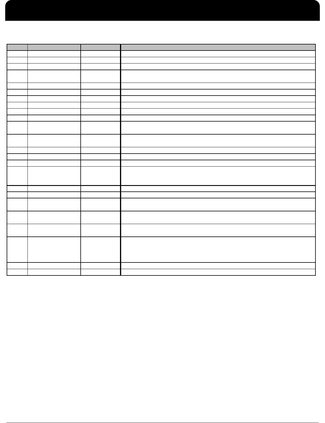
Absolute Maximum Ratings
Stresses above the ratings listed below can cause permanent damage to the 9DB833. These ratings, which are standard
values for IDT commercially rated parts, are stress ratings only. Functional operation of the device at these or any other
conditions above those indicated in the operational sections of the specifications is not implied. Exposure to absolute
maximum rating conditions for extended periods can affect product reliability. Electrical parameters are guaranteed only over
the recommended operating temperature range.
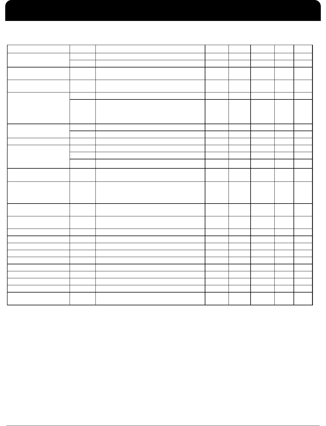
Electrical Characteristics–DIF_IN Clock Input Parameters
Electrical Characteristics–Current Consumption
PARAMETER SYMBOL CONDITIONS
MIN TYP MAX
UNITS NOTES
3.3V Core Supply Voltage VDDA/R 4.6 V 1,2
3.3V Logic Supply Voltage VDD 4.6 V
1,2
Input Low Voltage V
IL
GND-0.5 V 1
Input High Voltage V
IH
Except for SMBus interface V
DD
+0.5V V 1
Input High Voltage V
IHSMB
SMBus clock and data pins 5.5V V 1
Storage Temperature Ts -65 150
°
C
1
Junction Temperature Tj 125 °C
1
Input ESD protection
ESD prot Human Body Model 2000 V 1
1
Guaranteed by design and characterization, not 100% tested in production.
2
Operation under these conditions is neither implied nor
g
uaranteed.
T
AMB
=T
COM
or T
IND
unless otherwise indicated, Supply Voltages per normal operation conditions, See Test Loads for Loading Conditions
PARAMETER SYMBOL CONDITIONS MIN TYP MAX UNITS NOTES
Input Crossover Voltage -
DIF_IN
V
CROSS
Cross Over Voltage 150 375 900 mV 1
Input Swing - DIF_IN V
SWING
Differential value 300 mV 1
Input Slew Rate - DIF_IN dv/dt Measured differentially 1 8 V/ns 1,2
Input Leakage Current I
IN
V
IN
= V
DD ,
V
IN
=
GND -5 5 uA
Input Duty Cycle d
tin
Measurement from differential wavefrom 45 55 % 1
Input Jitter - Cycle to Cycle J
DIFIn
Differential Measurement 0 125 ps 1
1
Guaranteed by desi
g
n and characterization, not 100% tested in production.
2
Slew rate measured throu
g
h +/-75mV window centered around differential zero
TA = T
COM
or T
IND;
Supply Voltage VDD = 3.3 V +/-5%
PARAMETER SYMBOL CONDITIONS MIN TYP MAX UNITS NOTES
Operating Supply Current I
DD3.3OP
All outputs active @100MHz, PLL Mode,
C
L
= Full load;
164 200 mA 1
I
DD3.3PD
All diff pairs driven 53 60 mA 1
I
DD3.3PDZ
All differential pairs tri-stated 3 6 mA 1
1
Guaranteed by design and characterization, not 100% tested in production.
Powerdown Current
9DB833
EIGHT OUTPUT DIFFERENTIAL BUFFER FOR PCIE GEN1,2,3
IDT®
EIGHT OUTPUT DIFFERENTIAL BUFFER FOR PCIE GEN1,2,3 6
9DB833 REV H 06/07/16
Electrical Characteristics–Input/Supply/Common Parameters
PARAMETER SYMBOL CONDITIONS MIN TYP MAX UNITS NOTES
T
COM
Commmercial range 0 70 °C 1
T
IND
Industrial range -40 85 °C 1
Input High Voltage V
IH
Single-ended inputs, except SMBus, low
threshold and tri-level inputs
2V
DD
+ 0.3 V 1
Input Low Voltage V
IL
Single-ended inputs, except SMBus, low
threshold and tri-level inputs
GND
- 0.3 0.8 V 1
I
IN
Single-ended inputs, V
IN
= GND, V
IN
= VDD -5 -0.02 5 uA 1
I
INP
Single-ended inputs
V
IN
= 0 V; Inputs with internal pull-up resistors
V
IN
= VDD; Inputs with internal pull-down resistors
-50 50 uA 1
F
ib
yp
V
DD
= 3.3 V, Bypass mode 5 166 MHz 2
F
i
p
ll
V
DD
= 3.3 V, 100MHz PLL mode 50 100 110 MHz 2
Pin Inductance L
p
in
7nH1
C
IN
Logic Inputs, except DIF_IN 1.5 5 pF 1
C
INDIF_IN
DIF_IN differential clock inputs 1.5 2.7 pF 1,4
C
OUT
Output pin capacitance 6 pF 1
Clk Stabilization T
STAB
From V
DD
Power-Up and after input clock
stabilization or de-assertion of PD# to 1st clock
1ms1,2
Input SS Modulation
Frequency
f
MODI N
Allowable Frequency
(Triangular Modulation)
30 31.5 33 kHz 1
OE# Latency t
LATOE#
DIF start after OE# assertion
DIF stop after OE# deassertion
123cycles1,3
Tdrive_PD# t
DRVPD
DIF output enable after
PD# de-assertion
13 300 us 1,3
Tfall t
F
Fall time of control inputs 5 ns 1,2
Trise t
R
Rise time of control inputs 5 ns 1,2
SMBus Input Low Voltage V
ILSMB
0.8 V 1
SMBus Input High Voltage V
IHSMB
2.1 V
DDSMB
V1
SMBus Output Low Voltage V
OLSMB
@ I
PULLUP
0.4 V 1
SMBus Sink Current I
PULLUP
@ V
OL
4mA1
Nominal Bus Voltage V
DDSMB
3V to 5V +/- 10% 2.7 5.5 V 1
SCLK/SDATA Rise Time t
RSMB
(Max VIL - 0.15) to (Min VIH + 0.15) 1000 ns 1
SCLK/SDATA Fall Time t
FSMB
(Min VIH + 0.15) to (Max VIL - 0.15) 300 ns 1
SMBus Operating
Frequency
f
MAXSMB
Maximum SMBus operating frequency 440 kHz 1,5
1
Guaranteed by design and characterization, not 100% tested in production.
2
Control input must be monotonic from 20% to 80% of input swing.
5
The differential input clock must be running for the SMBus to be active
Ambient Operating
Temperature
Input Current
3
Time from deassertion until outputs are >200 mV
4
DIF_IN input
Capacitance
Input Frequency

9DB833AGILF

Mfr. #:
Manufacturer:
IDT
Description:
Clock Buffer 8 OUTPUT PCIE GEN3 BUFFER
Lifecycle:
New from this manufacturer.
Delivery:
DHL FedEx Ups TNT EMS
Payment:
T/T Paypal Visa MoneyGram Western Union