9DB833
EIGHT OUTPUT DIFFERENTIAL BUFFER FOR PCIE GEN1,2,3
IDT®
EIGHT OUTPUT DIFFERENTIAL BUFFER FOR PCIE GEN1,2,3 13
9DB833 REV H 06/07/16
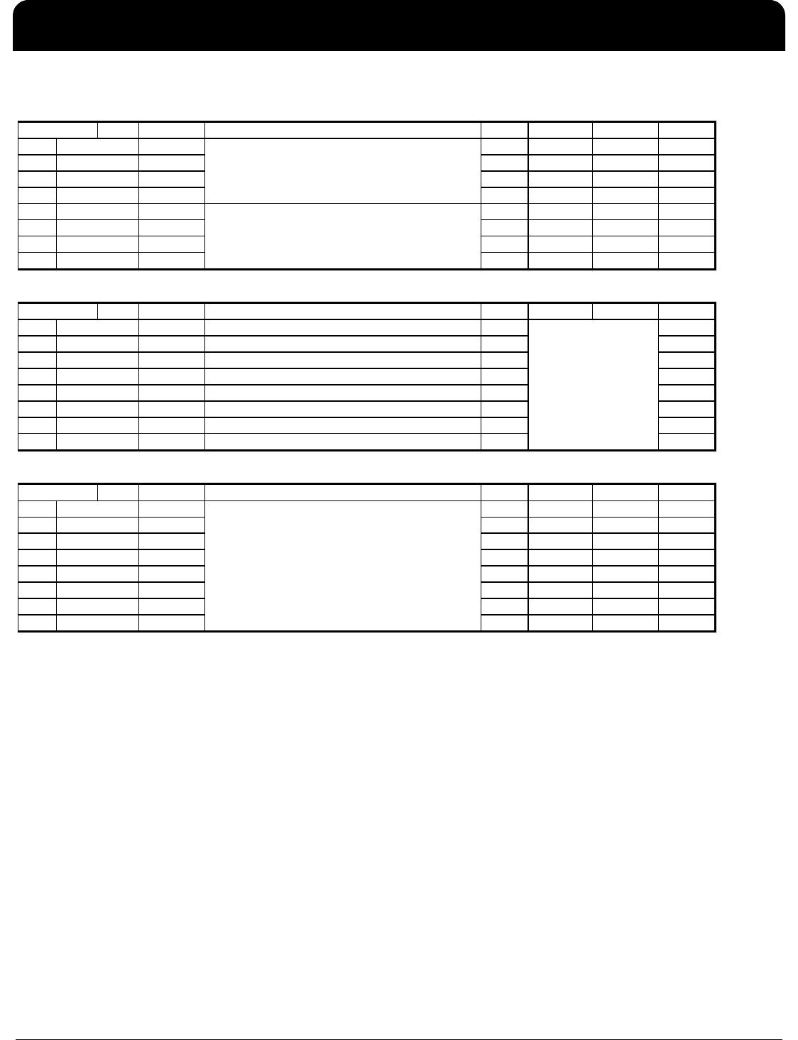
SMBus Table: Vendor & Revision ID Register
Pin # Name Control Function T
yp
e 0 1 Defaul
t
Bit 7
RID3 R - - 0
Bit 6
RID2 R - - 0
Bit 5
RID1 R - - 0
Bit 4
RID0 R - -
1
Bit 3
VID3 R - - 0
Bit 2
VID2 R - - 0
Bit 1
VID1 R - - 0
Bit 0
VID0 R - - 1
SMBus Table: DEVICE ID
Pin # Name Control Function T
yp
e 0 1 Defaul
t
Bit 7
DID7 Device ID 7 (MSB) RW 1
Bit 6
DID6 Device ID 6 RW 0
Bit 5
DID5 Device ID 5 RW 0
Bit 4
DID4 Device ID 4 RW 0
Bit 3
DID3 Device ID 3 RW 0
Bit 2
DID2 Device ID 2 RW 0
Bit 1
DID1 Device ID 1 RW 1
Bit 0
DID0 Device ID 0 RW 1
SMBus Table: Byte Count Register
Pin # Name Control Function T
yp
e 0 1 Defaul
t
Bit 7
BC7 RW - - 0
Bit 6
BC6 RW - - 0
Bit 5
BC5 RW - - 0
Bit 4
BC4 RW - - 0
Bit 3
BC3 RW - - 0
Bit 2
BC2 RW - - 1
Bit 1
BC1 RW - - 1
Bit 0
BC0 RW - - 1
REVISION ID
-
-
-
B
y
te 4
-
-
-
-
-
VENDOR ID
-
-
-
Device ID is 83 Hex
for 9DB833
B
y
te 5
-
Writing to this register configures how many
bytes will be read back.
-
-
-
-
-
-
-
B
y
te 6
-
-
-
-
-
9DB833
EIGHT OUTPUT DIFFERENTIAL BUFFER FOR PCIE GEN1,2,3
IDT®
EIGHT OUTPUT DIFFERENTIAL BUFFER FOR PCIE GEN1,2,3 14
9DB833 REV H 06/07/16
PD#, Power Down
The PD# pin cleanly shuts off all clocks and places the device into a power saving mode. PD# must be asserted before
shutting off the input clock or power to insure an orderly shutdown. PD is asynchronous active-low input for both powering
down the device and powering up the device. When PD# is asserted, all clocks will be driven high, or tri-stated (depending
on the PD# drive mode and Output control bits) before the PLL is shut down.
PD# Assertion
When PD# is sampled low by two consecutive rising edges of DIF#, all DIF outputs must be held High, or tri-stated
(depending on the PD# drive mode and Output control bits) on the next High-Low transition of the DIF# outputs. When the
PD# drive mode bit is set to ‘0’, all clock outputs will be held with DIF driven High with 2 x I
REF
and DIF# tri-stated. If the PD#
drive mode bit is set to ‘1’, both DIF and DIF# are tri-stated.
PD# De-assertion
Power-up latency is less than 1 ms. This is the time from de-assertion of the PD# pin, or VDD reaching 3.3V, or the time from
valid SRC_IN clocks until the time that stable clocks are output from the device (PLL Locked). If the PD# drive mode bit is
set to ‘1’, all the DIF outputs must driven to a voltage of >200 mV within 300 µs of PD# de-assertion.
9DB833
EIGHT OUTPUT DIFFERENTIAL BUFFER FOR PCIE GEN1,2,3
IDT®
EIGHT OUTPUT DIFFERENTIAL BUFFER FOR PCIE GEN1,2,3 15
9DB833 REV H 06/07/16
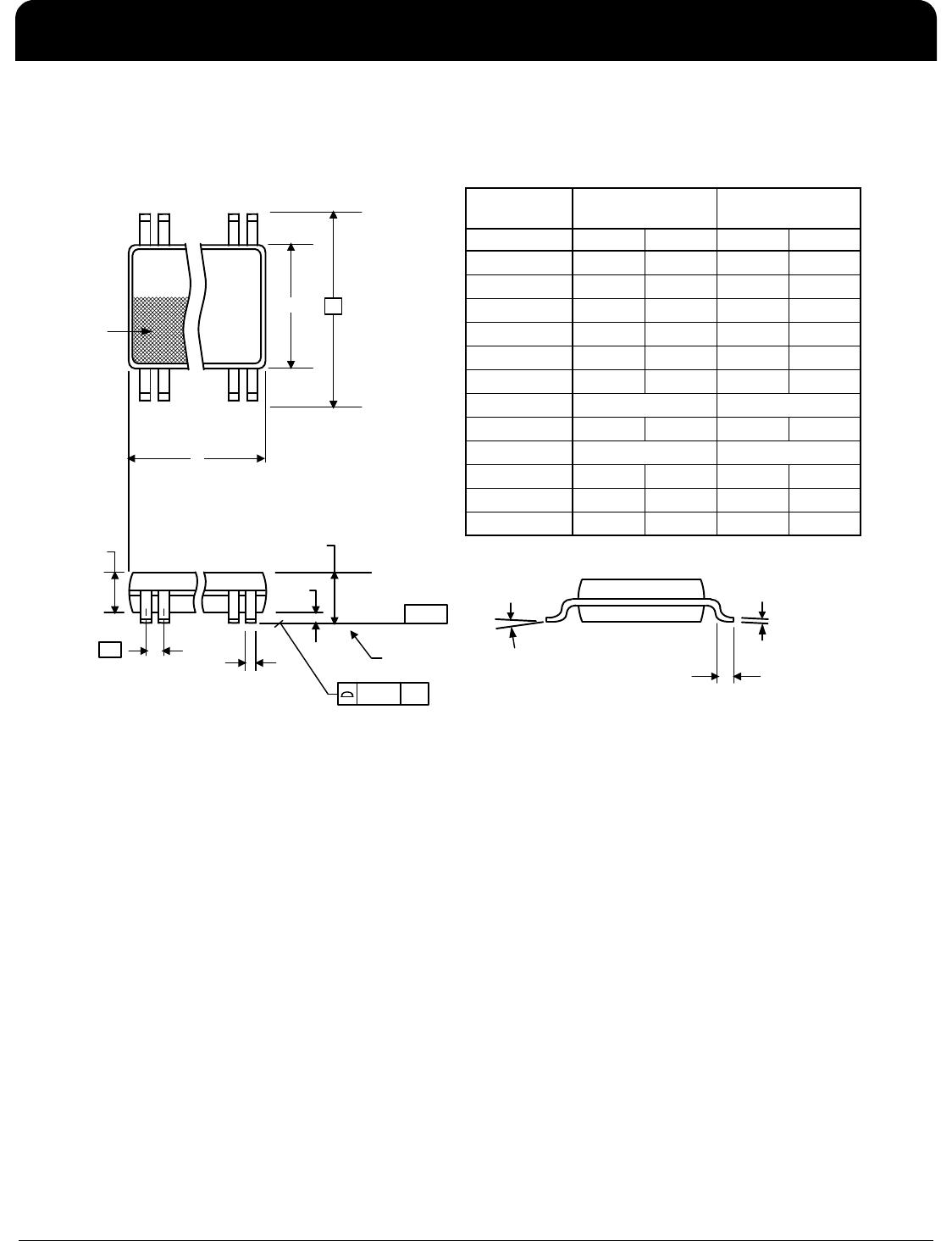
Package Outline and Package Dimensions (48-pin TSSOP)
Package dimensions are kept current with JEDEC Publication No. 95
INDEX
AREA
1 2
48
D
E1
E
SEATING
PLANE
A1
A
A2
e
- C -
b
aaa C
c
L
*For reference only. Controlling dimensions in mm.
Millimeters Inches*
Symbol Min Max Min Max
A--1.20--0.047
A1 0.05 0.15 0.002 0.006
A2 0.80 1.05 0.032 0.041
b 0.17 0.27 0.007 0.011
c 0.09 0.20 0.0035 0.008
D 12.40 12.60 0.488 0.496
E 8.10 BASIC 0.319 BASIC
E1 6.00 6.20 0.236 0.244
e 0.50 Basic 0.020 Basic
L 0.45 0.75 0.018 0.030
0 8 0 8
aaa -- 0.10 -- 0.004

9DB833AGILF

Mfr. #:
Manufacturer:
IDT
Description:
Clock Buffer 8 OUTPUT PCIE GEN3 BUFFER
Lifecycle:
New from this manufacturer.
Delivery:
DHL FedEx Ups TNT EMS
Payment:
T/T Paypal Visa MoneyGram Western Union