15 MHz Rail-to-Rail
Operational Amplifiers
Data Sheet
OP162/OP262/OP462
Rev. H Document Feedback
Information
furnished by Analog Devices is believed to be accurate and reliable. However, no
responsibility is assumed by Analog Devices for its use, nor for any infringements of patents or other
rights of third parties that may result from its use. Specifications subject to change without notice. No
license is granted by implication or otherwise under any patent or patent rights of Analog Devices.
Trademarks and registered trademarks are the property of their respective owners.
One Technology Way, P.O. Box 9106, Norwood, MA 02062-9106, U.S.A.
Tel: 781.329.4700 ©2013 Analog Devices, Inc. All rights reserved.
Technical Support www.analog.com
FEATURES
Wide bandwidth: 15 MHz
Low offset voltage: 325 µV max
Low noise: 9.5 nV/√
Hz
@ 1 kHz
Single-supply operation: 2.7 V to 12 V
Rail-to-rail output swing
Low TCV
OS
: 1 µVC typ
High slew rate: 13 V/µs
No phase inversion
Unity-gain stable
APPLICATIONS
Portable instrumentation
Sampling ADC amplifier
Wireless LANs
Direct access arrangement
Office automation
GENERAL DESCRIPTION
The OP162 (single), OP262 (dual), and OP462 (quad) rail-to-
rail 15 MHz amplifiers feature the extra speed new designs
require, with the benefits of precision and low power operation.
With their incredibly low offset voltage of 45 µV (typical) and
low noise, they are perfectly suited for precision filter applica-
tions and instrumentation. The low supply current of 500 µA
(typical) is critical for portable or densely packed designs. In
addition, the rail-to-rail output swing provides greater dynamic
range and control than standard video amplifiers.
These products operate from single supplies as low as 2.7 V to
dual supplies of ±6 V. The fast settling times and wide output
swings recommend them for buffers to sampling A/D converters.
The output drive of 30 mA (sink and source) is needed for
many audio and display applications; more output current can
be supplied for limited durations. The OPx62 family is specified
over the extended industrial temperature range (40°C to
+125°C). The single OP162 amplifiers are available in 8-lead
SOIC package. The dual OP262 amplifiers are available in
8-lead SOIC and TSSOP packages. The quad OP462 amplifiers
are available in 14-lead, narrow-body SOIC and TSSOP
packages.
PIN CONFIGURATIONS
Figure 1. 8-Lead Narrow-Body SOIC (S Suffix)
Figure 2. 8-Lead TSSOP (RU Suffix) and
8-Lead Narrow-Body SOIC (S Suffix)
Figure 3. 14-Lead Narrow-Body SOIC (S Suffix) and
14-Lead TSSOP (RU Suffix)
NULL
1
–IN A
2
+IN A
3
V–
4
NULL
8
V+
7
OUT A
6
NC
5
NC = NO CONNECT
OP162
TOP VIEW
(Not to Scale)
00288-001
TOP VIEW
(Not to Scale)
1
2
3
4
OP262
–IN A
+IN A
V–
OUT A
8
7
6
5
OUT B
–IN B
+IN B
V+
00288-004
1
2
3
4
5
6
7
OP462
–IN A
+IN A
V+
OUT B
–IN B
+IN B
OUT A
14
13
12
11
10
9
8
–IN D
+IN D
V–
OUT C
–IN C
+IN C
OUT D
TOP VIEW
(Not to Scale)
00288-006
OP162/OP262/OP462 Data Sheet
Rev. H | Page 2 of 20
TABLE OF CONTENTS
Features .............................................................................................. 1
Applications ....................................................................................... 1
General Description ......................................................................... 1
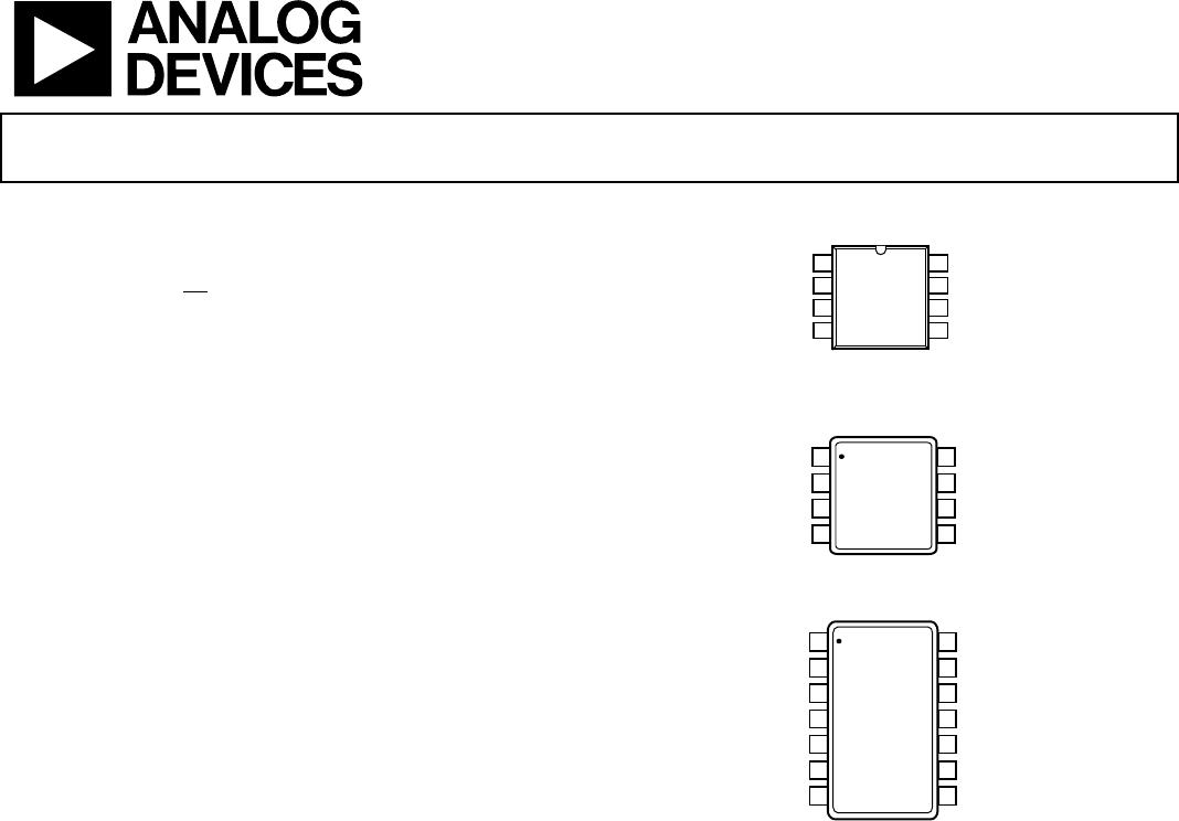
Pin Configurations ........................................................................... 1
Revision History ............................................................................... 2
Specifications ..................................................................................... 3
Absolute Maximum Ratings ............................................................ 6
ESD Caution .................................................................................. 6
Typical Performance Characteristics ............................................. 7
Applications ..................................................................................... 12
Functional Description .............................................................. 12
Offset Adjustment ...................................................................... 12
Rail-to-Rail Output .................................................................... 12
Output Short-Circuit Protection .............................................. 12
Input Overvoltage Protection ................................................... 13
Output Phase Reversal ............................................................... 13
Power Dissipation....................................................................... 13
Unused Amplifiers ..................................................................... 14
Power-On Settling Time ............................................................ 14
Capacitive Load Drive ............................................................... 14
Total Harmonic Distortion and Crosstalk .............................. 15
PCB Layout Considerations ...................................................... 15
Applications Circuits ...................................................................... 16
Single-Supply Stereo Headphone Driver................................. 16
Instrumentation Amplifier........................................................ 16
Direct Access Arrangement ...................................................... 17
Outline Dimensions ....................................................................... 18
Ordering Guide .......................................................................... 20
REVISION HISTORY
4/13—Rev. G to Rev. H
Combined Figure 2 and Figure 3; Combined Figure 4 and
Figure 5 .............................................................................................. 1
Changes to Figure 12 ........................................................................ 9
5/12Rev. F to Rev. G
Deleted MSOP Throughout ............................................................ 1
Deleted Figure 2; Renumbered Sequentially................................. 1
Deleted Spice-Macro Model Section ............................................ 18
Updated Outline Dimensions ....................................................... 18
Changes to Ordering Guide .......................................................... 20
1/05Rev. E to Rev. F
Changes to Absolute Maximum Ratings Table 4 and Table 5 .... 6
Change to Figure 36 ....................................................................... 13
Changes to Ordering Guide .......................................................... 20
12/04Rev. D to Rev. E
Updated Format .................................................................. Universal
Changes to General Description ..................................................... 1
Changes to Specifications ................................................................. 3
Changes to Package Type ................................................................. 6
Change to Figure 16 .......................................................................... 8
Change to Figure 22 .......................................................................... 9
Change to Figure 36 ....................................................................... 13
Change to Figure 37 ....................................................................... 14
Changes to Ordering Guide .......................................................... 20
10/02Rev. C to Rev. D
Deleted 8-Lead Plastic DIP (N-8) .................................... Universal
Deleted 14-Lead Plastic DIP (N-14) ................................ Universal
Edits to ORDERING GUIDE ....................................................... 19
Edits to Figure 30 ............................................................................ 19
Edits to Figure 31 ............................................................................ 19
Updated Outline Dimensions ....................................................... 19
Data Sheet OP162/OP262/OP462
Rev. H | Page 3 of 20
SPECIFICATIONS
@ V
S
= 5.0 V, V
CM
= 0 V, T
A
= 25°C, unless otherwise noted.
Table 1. Electrical Characteristics
Parameter Symbol Conditions Min Typ Max Unit
INPUT CHARACTERISTICS
Offset Voltage V
OS
OP162G, OP262G, OP462G 45 325 µV
40°C ≤ T
A
+125°C 800 µV
H grade, 40°C ≤ T
A
≤ +125°C 1 mV
D grade 0.8 3 mV
40°C ≤ T
A
≤ +125°C 5 mV
Input Bias Current
I
B
360
600
nA
40°C ≤ T
A
+125°C 650 nA
Input Offset Current I
OS
±2.5 ±25 nA
40°C ≤ T
A
+125°C ±40 nA
Input Voltage Range V
CM
0 4 V
Common-Mode Rejection CMRR 0 V ≤ V
CM
4.0 V,40°C ≤ T
A
+125°C 70 110 dB
Large Signal Voltage Gain A
VO
R
L
= 2 , 0.5 ≤ V
OUT
4.5 V 30 V/mV
R
L
= 10 , 0.5 ≤ V
OUT
4.5 V 65 88 V/mV
R
L
= 10 , 40°C ≤ T
A
≤ +125°C 40 V/mV
Long-Term Offset Voltage
1
V
OS
G grade 600 µV
Offset Voltage Drift
2
V
OS
/T
1 µV/°C
Bias Current Drift
I
B
/
T
250 pA/°C
OUTPUT CHARACTERISTICS
Output Voltage Swing High V
OH
I
L
= 250 µA, 40°C ≤ T
A
+125°C 4.95 4.99 V
I
L
= 5 mA 4.85 4.94 V
Output Voltage Swing Low V
OL
I
L
= 250 µA, 40°C ≤T
A
≤ +125°C 14 50 mV
I
L
= 5 mA 65 150 mV
Short-Circuit Current I
SC
Short to ground ±80 mA
Maximum Output Current I
OUT
±30 mA
POWER SUPPLY
Power Supply Rejection Ratio PSRR V
S
= 2.7 V to 7 V 120 dB
40°C ≤ T
A
≤ +125°C 90 dB
Supply Current/Amplifier I
SY
OP162, V
OUT
= 2.5 V 600 750 µA
40°C ≤ T
A
≤ +125°C 1 mA
OP262, OP462, V
OUT
= 2.5 V 500 700 µA
40°C ≤ T
A
≤ +125°C 850 µA
DYNAMIC PERFORMANCE
Slew Rate SR 1 V < V
OUT
< 4 V, R
L
= 10 kΩ 10 V/µs
Settling Time t
S
To 0.1%, A
V
= 1, V
O
= 2 V step 540 ns
Gain Bandwidth Product GBP 15 MHz
Phase Margin φ
m
61 Degrees
NOISE PERFORMANCE
Voltage Noise e
n
p-p 0.1 Hz to 10 Hz 0.5 µV p-p
Voltage Noise Density
e
n
f = 1 kHz
9.5
nV/√
Hz
Current Noise Density i
n
f = 1 kHz 0.4
pA/√
Hz
1
Long-term offset voltage is guaranteed by a 1000 hour life test performed on three independent lots at 125°C, with an LTPD of 1.3.
2
Offset voltage drift is the average of the −40°C to +25°C delta and the +25°C to +125°C delta.

OP162GSZ-REEL7

Mfr. #:
Manufacturer:
Analog Devices Inc.
Description:
Operational Amplifiers - Op Amps 15 MHZ RR SGL IC
Lifecycle:
New from this manufacturer.
Delivery:
DHL FedEx Ups TNT EMS
Payment:
T/T Paypal Visa MoneyGram Western Union