OP162/OP262/OP462 Data Sheet
Rev. H | Page 16 of 20
APPLICATIONS CIRCUITS
SINGLE-SUPPLY STEREO HEADPHONE DRIVER
Figure 43 shows a stereo headphone output amplifier that can
operate from a single 5 V supply. The reference voltage is
derived by dividing the supply voltage down with two 100 kΩ
resistors. A 10 µF capacitor prevents power supply noise from
contaminating the audio signal and establishes an ac ground for
the volume control potentiometers.
The audio signal is ac-coupled to each noninverting input
through a 10 µF capacitor. The gain of the amplifier is con-
trolled by the feedback resistors and is (R2/R1) + 1. For this
example, the gain is 6. By removing R1, the amplifier would
have unity gain. To short-circuit protect the output of the
device, a 169 Ω resistor is placed at the output in the feedback
network. This prevents any damage to the device if the head-
phone output becomes shorted. A 270 µF capacitor is used at
the output to couple the amplifier to the headphone. This value
is much larger than that used for the input because of the low
impedance of headphones, which can range from 32 Ω to 600 Ω
or more.
Figure 43. Headphone Output Amplifier
INSTRUMENTATION AMPLIFIER
Because of their high speed, low offset voltages, and low noise
characteristics, the OP162/OP262/OP462 can be used in a wide
variety of high speed applications, including precision instru-
mentation amplifiers. Figure 44 shows an example of such an
application.
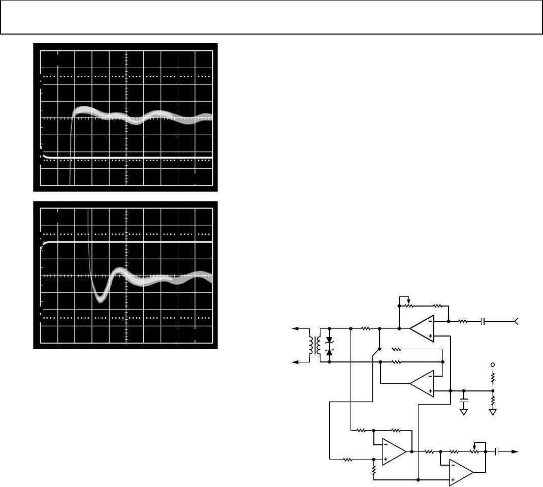
Figure 44. High Speed Instrumentation Amplifier
The differential gain of the circuit is determined by R
G
, where
with the R
G
resistor value in kΩ. Removing R
G
sets the circuit
gain to unity.
The fourth op amp, OP462-D, is optional and is used to
improve CMRR by reducing any input capacitance to the
amplifier. By shielding the input signal leads and driving the
shield with the common-mode voltage, input capacitance is
eliminated at common-mode voltages. This voltage is derived
from the midpoint of the outputs of OP462-A and OP462-B by
using two 10 kΩ resistors followed by OP462-D as a unity-gain
buffer.
It is important to use 1% or better tolerance components for the
2 kΩ resistors, as the common-mode rejection is dependent on
their ratios being exact. A potentiometer should also be connected
in series with the OP462-C noninverting input resistor to ground
to optimize common-mode rejection.
The circuit in Figure 44 was implemented to test its settling
time. The instrumentation amp was powered with −5 V, so the
input step voltage went from −5 V to +4 V to keep the OP462
within its input range. Therefore, the 0.05% settling range is
when the output is within 4.5 mV. Figure 45 shows the positive
slope settling time to be 1.8 µs, and Figure 46 shows a settling
time of 3.9 µs for the negative slope.
OP262-A
5V
169Ω
270µ
F
47kΩ
L VOLUME
CONTROL
R1 = 10kΩ
10
µF
1
0µF
10k
Ω
5V
100kΩ
10µF
100kΩ
R2 = 50kΩ
LEFT IN
OP262-B
5V
169Ω
270µF
47kΩ
HEADPHONE
RIGHT
HEADPHONE
LEFT
10k
Ω
R VOLUME
CONTROL
10
µF
RIGHT IN
R2 = 50k
Ω
10µ
F
R1 = 10kΩ
00288-046
OP462-A
OP462-B
OP462-C
OP462-D
–
V
IN
+V
IN
1kΩ
10k
Ω
2kΩ
1.9kΩ
200Ω
10 TURN
(OPTIONAL)
OUTPUT
R
G
1k
Ω
10k
Ω
2kΩ
2k
Ω
00288-047