Data Sheet OP162/OP262/OP462
Rev. H | Page 13 of 20
and V
IN
swings up to 5 V, the output current will not exceed
30 mA. For single 5 V supply applications, resistors less than
169are not recommended.
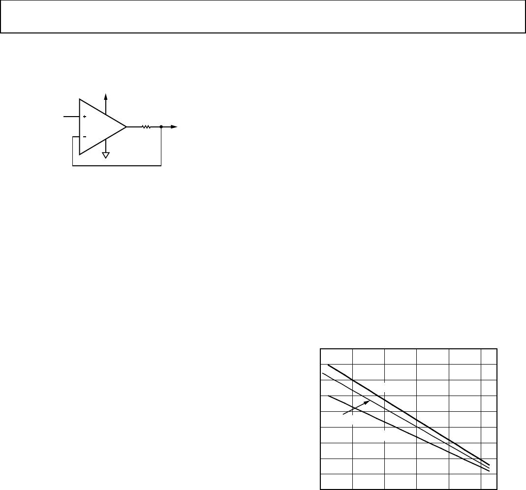
Figure 32. Output Short-Circuit Protection
INPUT OVERVOLTAGE PROTECTION
The input voltage should be limited to ±6 V, or damage to the
device can occur. Electrostatic protection diodes placed in the
input stage of the device help protect the amplifier from static
discharge. Diodes are connected between each input as well as
from each input to both supply pins as shown in the simplified
equivalent circuit in Figure 30. If an input voltage exceeds either
supply voltage by more than 0.6 V, or if the differential input
voltage is greater than 0.6 V, these diodes energize causing
overvoltage damage.
The input current should be limited to less than 5 mA to
prevent degradation or destruction of the device by placing an
external resistor in series with the input at risk of being overdriven.
The size of the resistor can be calculated by dividing the maxi-
mum input voltage by 5 mA. For example, if the differential
input voltage could reach 5 V, the external resistor should be
5 V/5 mA = 1 kΩ. In practice, this resistor should be placed in
series with both inputs to balance any offset voltages created by
the input bias current.
OUTPUT PHASE REVERSAL
The OP162/OP262/OP462 are immune to phase reversal as
long as the input voltage is limited to ±6 V. Figure 27 shows the
output of a device with the input voltage driven beyond the
supply voltages. Although the devices output does not change
phase, large currents due to input overvoltage could result,
damaging the device. In applications where the possibility of an
input voltage exceeding the supply voltage exists, overvoltage
protection should be used, as described in the previous section.
POWER DISSIPATION
The maximum power that can be safely dissipated by the
OP162/OP262/OP462 is limited by the associated rise in
junction temperature. The maximum safe junction temperature
is 150°C; device performance suffers when this limit is
exceeded. If this maximum is only momentarily exceeded,
proper circuit operation will be restored as soon as the die
temperature is reduced. Leaving the device in an “overheated”
condition for an extended period can result in permanent
damage to the device.
To calculate the internal junction temperature of the OPx62, use
the formula
T
J
= P
DISS
× θ
JA
+ T
A
where:
T
J
is the OPx62 junction temperature.
P
DISS
is the OPx62 power dissipation.
θ
JA
is the OPx62 package thermal resistance, junction-to-
ambient temperature.
T
A
is the ambient temperature of the circuit.
The power dissipated by the device can be calculated as
P
DISS
= I
LOAD
× (V
S
V
OUT
)
where:
I
LOAD
is the OPx62 output load current.
V
S
is the OPx62 supply voltage.
V
OUT
is the OPx62 output voltage.
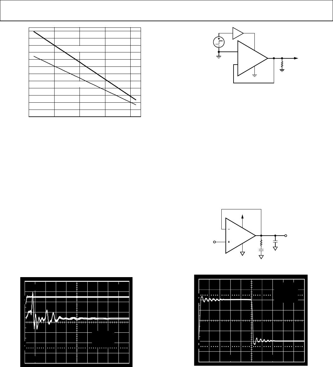
Figure 33 and Figure 34 provide a convenient way to determine
if the device is being overheated. The maximum safe power
dissipation can be found graphically, based on the package type
and the ambient temperature around the package. By using the
previous equation, it is a simple matter to see if P
DISS
exceeds the
device’s power derating curve. To ensure proper operation, it is
important to observe the recommended derating curves shown
in Figure 33 and Figure 34.
Figure 33. Maximum Power Dissipation vs. Temperature for
8-Lead Package Types
OPx62
V
IN
V
OUT
169
5V
00288-035
AMBIENT TEMPERATURE (°C)
MAXIMUM POWER DISSIPATION (Watts)
0.9
0.7
0.8
0.5
0.6
0.1
0.2
0.3
0.4
0
20 40 60 10080 120
00288-036
8-LEAD SOIC
8-LEAD MSOP
8-LEAD TSSOP
OP162/OP262/OP462 Data Sheet
Rev. H | Page 14 of 20
Figure 34. Maximum Power Dissipation vs. Temperature for
14-Lead Package Types
UNUSED AMPLIFIERS
It is recommended that any unused amplifiers in a dual or a
quad package be configured as a unity-gain follower with a
1 kΩ feedback resistor connected from the inverting input to
the output, and the noninverting input tied to the ground plane.
POWER-ON SETTLING TIME
The time it takes for the output of an op amp to settle after a
supply voltage is delivered can be an important consideration in
some power-up-sensitive applications. An example of this
would be in an A/D converter where the time until valid data
can be produced after power-up is important.
The OPx62 family has a rapid settling time after power-up.
Figure 35 shows the OP462 output settling times for a single-
supply voltage of V
S
= +5 V. The test circuit in Figure 36 was
used to find the power-on settling times for the device.
Figure 35. Oscilloscope Photo of V
S
and V
OUT
Figure 36. Test Circuit for Power-On Settling Time
CAPACITIVE LOAD DRIVE
The OP162/OP262/OP462 are high speed, extremely accurate
devices that tolerate some capacitive loading at their outputs. As
load capacitance increases, unity-gain bandwidth of an OPx62
device decreases. This also causes an increase in overshoot and
settling time for the output. Figure 38 shows an example of this
with the device configured for unity gain and driving a 10 k
resistor and 300 pF capacitor placed in parallel.
By connecting a series R-C network, commonly called a
“snubber network, from the output of the device to ground,
this ringing can be eliminated and overshoot can be
significantly reduced. Figure 37 shows how to set up the
snubber network, and Figure 39 shows the improvement in
output response with the network added.
Figure 37. Snubber Network Compensation for Capacitive Loads
Figure 38. A Photo of a Ringing Square Wave
AMBIENT TEMPERATURE (°C)
MAXIMUM POWER DISSIPATION (Watts)
0.3
0.4
0.5
0.6
0.7
0.8
0.9
1.0
1.1
1.2
0.1
0.2
0
20 45 70 95 120
00288-037
14-LEAD SOIC
14-LEAD TSSOP
10
0%
100
90
500n
s
2
V
50
mV
V
S
= 5V
A
V
= 1
R
L
= 10k
00288-038
OP462
V
OUT
0 TO +5V
SQUARE
10K
00288-039
1
OPx62
V
IN
V
OUT
R
X
C
X
C
L
5V
00288-040
00288-041
50mV s
100
90
10
0%
V
S
= 5V
A
V
= 1
C
L
= 300pF
R
L
= 10k
Data Sheet OP162/OP262/OP462
Rev. H | Page 15 of 20
Figure 39. A Photo of a Nice Square Wave at the Output
The network operates in parallel with the load capacitor, C
L
,
and provides compensation for the added phase lag. The actual
values of the network resistor and capacitor are empirically
determined to minimize overshoot and maximize unity-gain
bandwidth. Table 6 shows a few sample snubber networks for
large load capacitors.
Table 6. Snubber Networks for Large Capacitive Loads
C
LOAD
R
X
C
X
< 300 pF 140 Ω 10 nF
500 pF 100 Ω 10 nF
1 nF 80 Ω 10 nF
10 nF 10 Ω 47 nF
Higher load capacitance will reduce the unity-gain bandwidth
of the device. Figure 40 shows unity-gain bandwidth vs.
capacitive load. The snubber network does not provide any
increase in bandwidth, but it substantially reduces ringing and
overshoot, as shown between Figure 38 and Figure 39.
Figure 40. Unity-Gain Bandwidth vs. C
LOAD
TOTAL HARMONIC DISTORTION AND CROSSTALK
The OPx62 device family offers low total harmonic distortion
making it an excellent choice for audio applications. Figure 41
shows a graph of THD plus noise figures at 0.001% for the
OP462.
Figure 42 shows the worst case crosstalk between two amplifiers
in the OP462. A 1 V rms signal is applied to one amplifier while
measuring the output of an adjacent amplifier. Both amplifiers
are configured for unity gain and supplied with ±2.5 V.
Figure 41. THD + N vs. Frequency
Figure 42. Crosstalk vs. Frequency
PCB LAYOUT CONSIDERATIONS
Because the OP162/OP262/OP462 can provide gains at high
frequency, careful attention to board layout and component
selection is recommended. As with any high speed application,
a good ground plane is essential to achieve the optimum
performance. This can significantly reduce the undesirable
effects of ground loops and I × R losses by providing a low
impedance reference point. Best results are obtained with a
multilayer board design with one layer assigned to ground
plane.
Use chip capacitors for supply bypassing, with one end of the
capacitor connected to the ground plane and the other end
connected within 1/8 inch of each power pin. An additional
large tantalum electrolytic capacitor (4.7 µF to 10 µF) should be
connected in parallel. This capacitor provides current for fast,
large-signal changes at the devices output; therefore, it does not
need to be placed as close to the supply pins.
00288-042
10
0%
100
90
50mV
1µs
V
S
= 5V
A
V
= 1
C
L
= 300pF
R
L
= 10k
WITH SNUBBER:
R
X
= 140
C
X
= 10nF
C
LOAD
BANDWIDTH (MHz)
10
7
8
9
5
6
4
3
2
1
0
10pF 100pF 1nF 10nF
00288-043
FREQUENCY (Hz)
THD+N (%)
0.010
0.001
0.0001
20
100 1k
10k
20k
00288-044
V
S
= ±2.5V
A
V
= 1
V
IN
= 1.0V rms
R
L
= 10k
BANDWIDTH:
<10Hz TO 22kHz
FREQUENCY (Hz)
XTALK (dBV)
40
90
–80
–70
60
–50
–140
–130
–120
–110
–100
20
100 1k 10k
20k
00288-045
A
V
= 1
V
IN
= 1.0V rms
(0dBV)
R
L
= 10k
V
S
=
±2.5V

OP162GSZ-REEL7

Mfr. #:
Manufacturer:
Analog Devices Inc.
Description:
Operational Amplifiers - Op Amps 15 MHZ RR SGL IC
Lifecycle:
New from this manufacturer.
Delivery:
DHL FedEx Ups TNT EMS
Payment:
T/T Paypal Visa MoneyGram Western Union