35
COMMERCIAL AND INDUSTRIAL
TEMPERATURE RANGES
IDT72V36100/72V36110 3.3V HIGH DENSITY SUPERSYNC II
TM
36-BIT FIFO
65,536 x 36 and 131,072 x 36
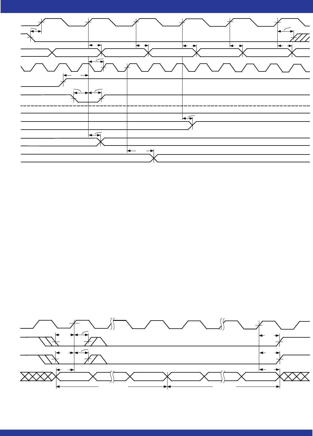
NOTES:
1. m = PAF offset.
2. D = maximum FIFO depth.
In IDT Standard mode: D = 65,536 for the IDT72V36100 and 131,072 for the IDT72V36110.
In FWFT mode: D = 65,537 for the IDT72V36100 and 131,073 for the IDT72V36110.
3.
t
SKEW2
is the minimum time between a rising RCLK edge and a rising WCLK edge to guarantee that PAF will go HIGH (after one WCLK cycle plus t
PAFS
). If the time between the
rising edge of RCLK and the rising edge of WCLK is less than t
SKEW2
, then the PAF deassertion time may be delayed one extra WCLK cycle.
4. PAF is asserted and updated on the rising edge of WCLK only.
5. Select this mode by setting PFM HIGH during Master Reset.
WCLK
WEN
PAF
RCLK
(3)
t
PAFS
REN
6117 drw 23
D - (m+1) words in FIFO
(2)
D - m words in FIFO
(2)
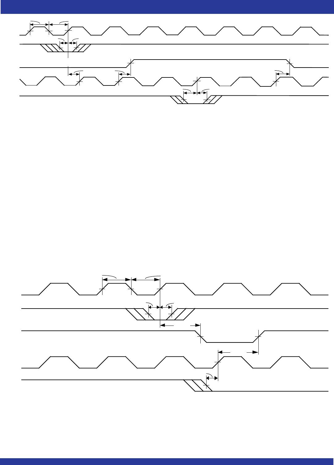
1
2
12
D-(m+1) words
in FIFO
(2)
t
PAFS
t
ENH
t
ENS
t
SKEW2
t
ENH
t
ENS
t
CLKL
t
CLKL
RCLK
LD
REN
Q
0
- Q
n
tLDH
tLDS
tENS
DATA IN OUTPUT REGISTER PAE OFFSET
PAF OFFSET
tENH
tENH
tLDH
6117 drw 22
t
CLK
tA
tA
tCLKH tCLKL
WCLK
LD
WEN
D
0 - Dn
6117 drw 21
t
LDS
t
ENS
PAE
OFFSET
PAF
OFFSET
t
DS
t
DH
t
LDH
t
ENH
t
CLK
t
LDH
t
ENH
t
DH
t
CLKH
t
CLKL
Figure 18. Synchronous Programmable Almost-Full Flag Timing (IDT Standard and FWFT Modes)
NOTES:
1. OE = LOW.
2. The timing diagram illustrates reading of offset registers with an output bus width of 36 bits.
Figure 17. Parallel Read of Programmable Flag Registers (IDT Standard and FWFT Modes)
Figure 16. Parallel Loading of Programmable Flag Registers (IDT Standard and FWFT Modes)
NOTE:
1. This timing diagram illustrates programming with an input bus width of 36 bits.