45
COMMERCIAL AND INDUSTRIAL
TEMPERATURE RANGES
IDT72V36100/72V36110 3.3V HIGH DENSITY SUPERSYNC II
TM
36-BIT FIFO
65,536 x 36 and 131,072 x 36
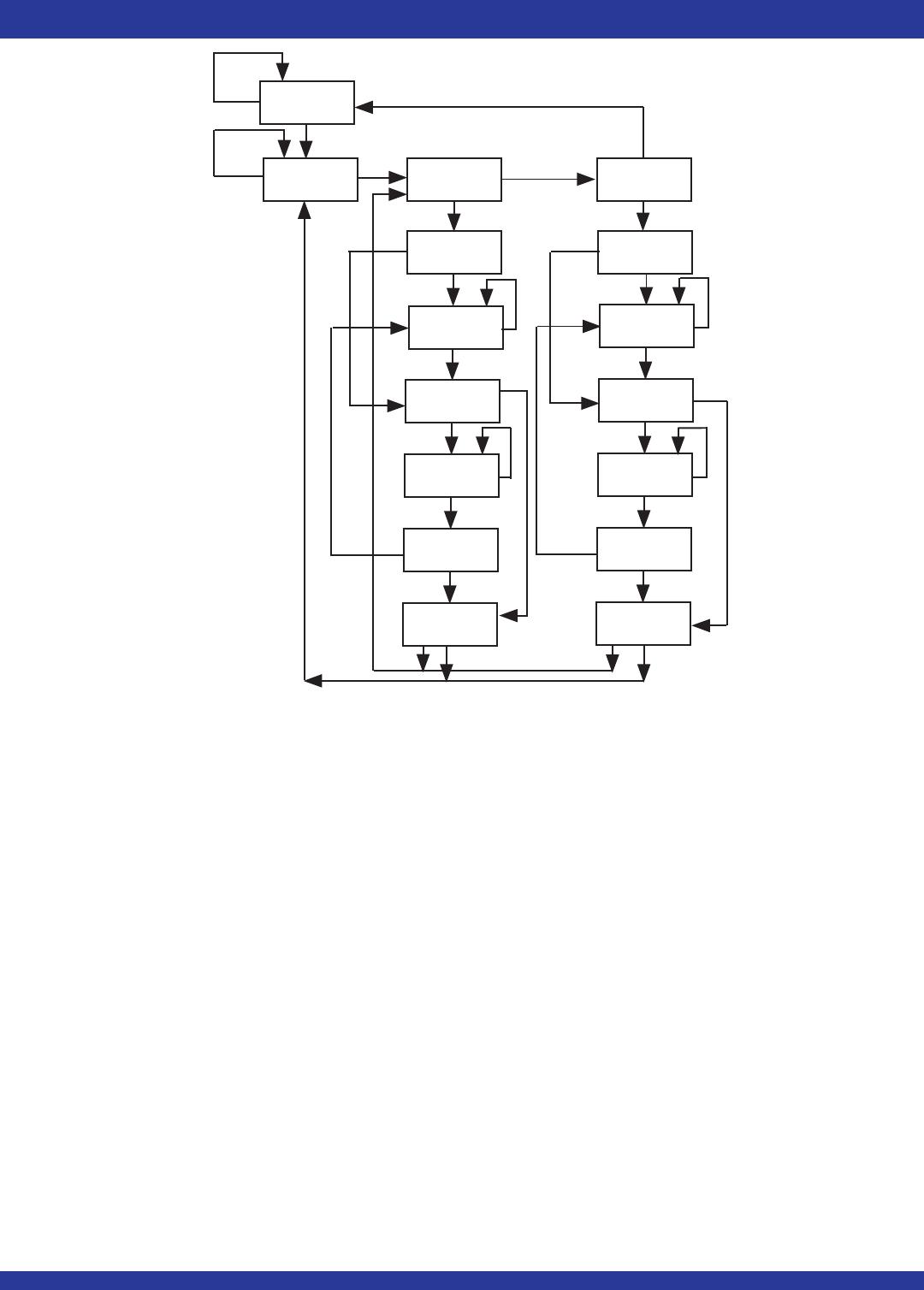
Figure 33. TAP Controller State Diagram
Test-Logic
Reset
Run-Test/
Idle
1
0
0
Select-
DR-Scan
Select-
IR-Scan
1
1
1
Capture-IR
0
Capture-DR
0
0
Exit1-DR
1
Pause-DR
0
Exit2-DR
1
Update-DR
1
Exit1-IR
1
Exit2-IR
1
Update-IR
1
1
0
1
1
1
6117 drw38
0
Shift-DR
0
0
0
Shift-IR
0
0
Pause-IR
0
1
Input = TMS
0
0
1
Refer to the IEEE Standard Test Access Port Specification (IEEE Std.
1149.1) for the full state diagram.
All state transitions within the TAP controller occur at the rising edge of the
TCLK pulse. The TMS signal level (0 or 1) determines the state progression
that occurs on each TCLK rising edge. The TAP controller takes precedence
over the Queue and must be reset after power up of the device. See TRST
description for more details on TAP controller reset.
Test-Logic-Reset All test logic is disabled in this controller state enabling
the normal operation of the IC. The TAP controller state machine is designed
in such a way that, no matter what the initial state of the controller is, the Test-
Logic-Reset state can be entered by holding TMS at high and pulsing TCK five
times. This is the reason why the Test Reset (TRST) pin is optional.
Run-Test-Idle In this controller state, the test logic in the IC is active only if
certain instructions are present. For example, if an instruction activates the self
test, then it will be executed when the controller enters this state. The test logic
in the IC is idles otherwise.
Select-DR-Scan This is a controller state where the decision to enter the
Data Path or the Select-IR-Scan state is made.
Select-IR-Scan This is a controller state where the decision to enter the
Instruction Path is made. The Controller can return to the Test-Logic-Reset state
other wise.
Capture-IR In this controller state, the shift register bank in the Instruction
Register parallel loads a pattern of fixed values on the rising edge of TCK. The
last two significant bits are always required to be “01”.
Shift-IR In this controller state, the instruction register gets connected
between TDI and TDO, and the captured pattern gets shifted on each rising edge
of TCK. The instruction available on the TDI pin is also shifted in to the instruction
register.
Exit1-IR This is a controller state where a decision to enter either the Pause-
IR state or Update-IR state is made.
Pause-IR This state is provided in order to allow the shifting of instruction
register to be temporarily halted.
Exit2-DR This is a controller state where a decision to enter either the Shift-
IR state or Update-IR state is made.
Update-IR In this controller state, the instruction in the instruction register is
latched in to the latch bank of the Instruction Register on every falling edge of
TCK. This instruction also becomes the current instruction once it is latched.
Capture-DR In this controller state, the data is parallel loaded in to the data
registers selected by the current instruction on the rising edge of TCK.
Shift-DR, Exit1-DR, Pause-DR, Exit2-DR and Update-DR These
controller states are similar to the Shift-IR, Exit1-IR, Pause-IR, Exit2-IR and
Update-IR states in the Instruction path.
NOTE:
1. Five consecutive TCK cycles with TMS = 1 will reset the TAP.

