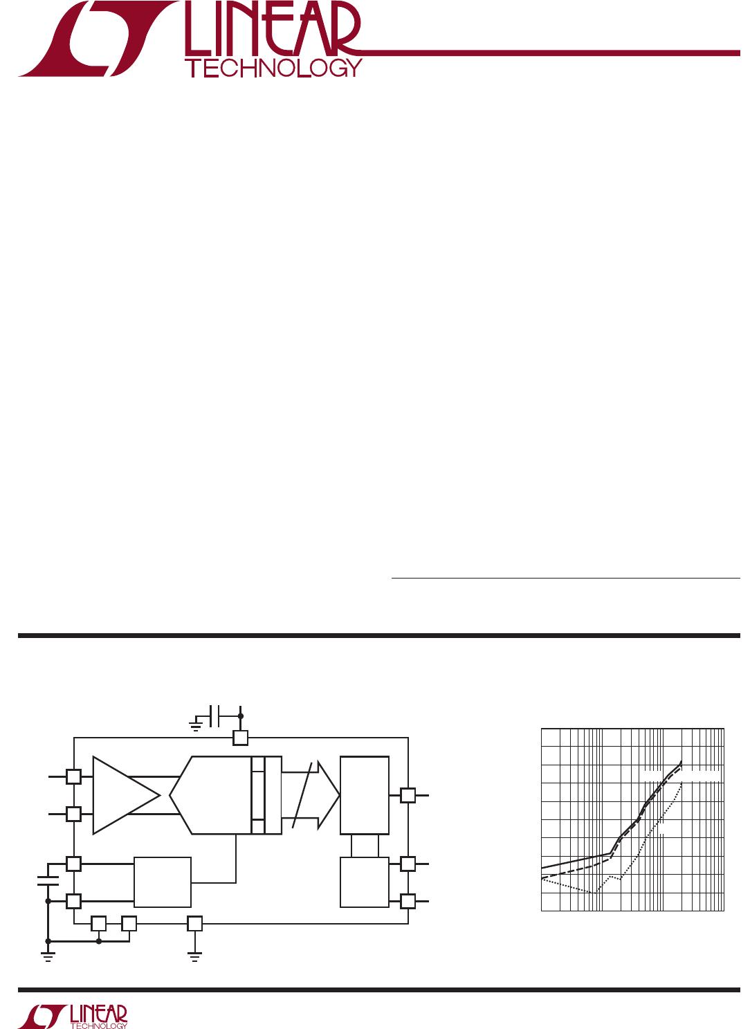
LTC1403/LTC1403A
1
1403fc
For more information www.linear.com/LTC1403
Block Diagram
Features
applications
Description
Serial 12-Bit/14-Bit, 2.8Msps
Sampling ADCs with Shutdown
The LT C
®
1403/LTC1403A are 12-bit/14-bit, 2.8Msps se-
rial ADCs with differential inputs. The devices draw only
4.7mA from a single
3V supply and come in a tiny 10-lead
MS package. A Sleep shutdown feature lowers power
consumption to 10µW. The combination of speed, low
power and tiny package makes the LTC1403/LTC1403A
suitable for high speed, portable applications.
The 80dB common mode rejection allows users to eliminate
ground loops and common mode noise by measuring
signals differentially from the source.
The devices convert 0V to 2.5V unipolar inputs differentially.
The absolute voltage swing for +A
IN
and –A
IN
extends from
ground to the supply voltage.
The serial interface sends out the conversion results during
the 16 clock cycles following CONV for compatibility with
standard serial interfaces. If two additional clock cycles
for acquisition time are allowed after the data stream in
between conversions, the full sampling rate of 2.8Msps
can be achieved with a 50.4MHz clock.
n
2.8Msps Conversion Rate
n
Low Power Dissipation: 14mW
n
3V Single Supply Operation
n
–40°C to 125°C Guaranteed Operation
n
2.5V Internal Bandgap Reference can be Overdriven
n
3-Wire Serial Interface
n
Sleep (10µW) Shutdown Mode
n
Nap (3mW) Shutdown Mode
n
80dB Common Mode Rejection
n
0V to 2.5V Unipolar Input Range
n
Tiny 10-Lead MS Package
n
Automotive
n
Communications
n
Data Acquisition Systems
n
Uninterrupted Power Supplies
n
Multiphase Motor Control
n
Multiplexed Data Acquisition
2nd, 3rd and SFDR vs
Input Frequency
L, LT, LTC, LTM, Linear Technology and the Linear logo are registered trademarks and
LinearView and SoftSpan are trademarks of Linear Technology Corporation. All other trademarks
are the property of their respective owners.
+
1
2
7
3
4
S & H
GND
EXPOSED PAD
LTC1403A
V
REF
10F
A
IN
A
IN
+
14-BIT ADC
3V10µF
14
14-BIT LATCH
8
10
9
THREE-
STATE
SERIAL
OUTPUT
PORT
2.5V
REFERENCE
TIMING
LOGIC
V
DD
SDO
CONV
SCK
1403A TA01
5 6 11
FREQUENCY (MHz)
0.1
–80
THD, 2nd, SFDR, 3rd (dB)
–74
–68
–62
–56
1 10 100
1403A TA02
–86
–92
–98
–104
–50
–44
THD
3rd
2nd, SFDR
LTC1403/LTC1403A
2
1403fc
For more information www.linear.com/LTC1403
pin conFigurationaBsolute maximum ratings
Supply Voltage (V
DD
) ..................................................4V
Analog Input Voltage
(Note 3) ................................... 0.3V to (V
DD
+ 0.3V)
Digital Input Voltage..................... 0.3V to (V
DD
+ 0.3V)
Digital Output Voltage .................. 0.3V to (V
DD
+ 0.3V)
Power Dissipation ...............................................100mW
Operation Temperature Range
LTC1403C/LTC1403AC ............................. 0°C to 70°C
LTC1403I/LTC1403AI ........................... 40°C to 85°C
LTC1403H/LTC1403AH ...................... 40°C to 125°C
Storage Temperature Range .................. 65°C to 150°C
Lead Temperature (Soldering, 10 sec) ...................300°C
(Note 1, 2,)
orDer inFormation
LEAD FREE FINISH TAPE AND REEL PART MARKING* PACKAGE DESCRIPTION TEMPERATURE RANGE
LTC1403CMSE#PBF LTC1403CMSE#TRPBF LTBDN 10-Lead Plastic MSOP 0°C to 70°C
LTC1403IMSE#PBF LTC1403IMSE#TRPBF LTBDP 10-Lead Plastic MSOP –40°C to 85°C
LTC1403HMSE#PBF LTC1403HMSE#TRPBF LTBDP 10-Lead Plastic MSOP –40°C to 125°C
LTC1403ACMSE#PBF LTC1403ACMSE#TRPBF LTADF 10-Lead Plastic MSOP 0°C to 70°C
LTC1403AIMSE#PBF LTC1403AIMSE#TRPBF LTAFD 10-Lead Plastic MSOP –40°C to 85°C
LTC1403AHMSE#PBF LTC1403AHMSE#TRPBF LTAFD 10-Lead Plastic MSOP –40°C to 125°C
Consult LTC Marketing for parts specified with wider operating temperature ranges. *The temperature grade is identified by a label on the shipping container.
For more information on lead free part marking, go to: http://www.linear.com/leadfree/
For more information on tape and reel specifications, go to: http://www.linear.com/tapeandreel/. Some packages are available in 500 unit reels through
designated sales channels with #TRMPBF suffix.
1
2
3
4
5
A
IN
+
A
IN
V
REF
GND
GND
10
9
8
7
6
CONV
SCK
SDO
V
DD
GND
TOP VIEW
11
GND
MSE PACKAGE
10-LEAD PLASTIC MSOP
T
JMAX
= 150°C, q
JA
= 40°C/W
EXPOSED PAD (PIN 11) IS GND
MUST BE SOLDERED TO PCB
http://www.linear.com/product/LTC1403#orderinfo
LTC1403/LTC1403A
3
1403fc
For more information www.linear.com/LTC1403
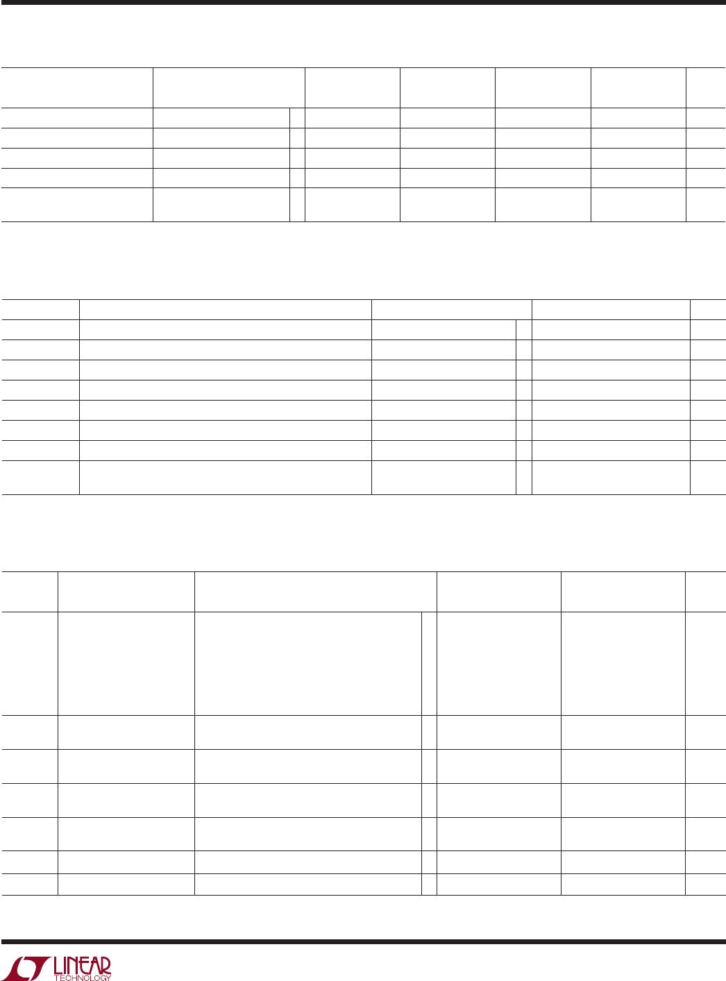
converter characteristics
PARAMETER CONDITIONS
LTC1403 LTC1403H LTC1403A LTC1403AH
UNITSMIN TYP MAX MIN TYP MAX MIN TYP MAX MIN TYP MAX
Resolution (No Missing Codes)
l
12 12 14 14 Bits
Integral Linearity Error (Notes 4, 5, 18)
l
–2 ±0.25 2 –2 ±0.25 2 –4 ±0.5 4 –4 ±0.5 4 LSB
Offset Error (Notes 4, 18)
l
–10 ±1 10 –20 ±2 20 –20 ±2 20 –30 ±2 30 LSB
Gain Error (Note 4, 18)
l
–30 ±5 30 –40 ±5 40 –60 ±10 60 –80 ±10 80 LSB
Gain Tempco Internal Reference (Note 4)
External Reference
±15
±1
±15
±1
±15
±1
±15
±1
ppm/°C
ppm/°C
The l denotes the specifications which apply over the full operating
temperature range, otherwise specifications are at T
A
= 25°C. With internal reference. V
DD
= 3V
SYMBOL PARAMETER CONDITIONS MIN TYP MAX UNITS
V
IN
Analog Differential Input Range (Notes 3, 9) 2.7V ≤ V
DD
≤ 3.3V
l
0 to 2.5 V
V
CM
Analog Common Mode + Differential Input Range (Note 10) 0 to V
DD
V
I
IN
Analog Input Leakage Current
l
1 µA
C
IN
Analog Input Capacitance 13 pF
t
ACQ
Sample-and-Hold Acquisition Time (Note 6)
l
39 ns
t
AP
Sample-and-Hold Aperture Delay Time 1 ns
t
JITTER
Sample-and-Hold Aperture Delay Time Jitter 0.3 ps
CMRR Analog Input Common Mode Rejection Ratio f
IN
= 1MHz, V
IN
= 0V to 3V
f
IN
= 100MHz, V
IN
= 0V to 3V
–60
–15
dB
dB
analog input
The l denotes the specifications which apply over the full operating temperature range, otherwise
specifications are at T
A
= 25°C. V
DD
= 3V
The
l denotes the specifications which apply over the full operating temperature range,
otherwise specifications are at T
A
= 25°C. V
DD
= 3V
Dynamic accuracy
SYMBOL PARAMETER CONDITIONS
LTC1403/LTC1403H LTC1403A/LTC1403AH
UNITSMIN TYP MAX MIN TYP MAX
SINAD Signal-to-Noise Plus
Distortion Ratio
100kHz Input Signal
1.4MHz Input Signal
1.4MHz Input Signal (H Grade)
100kHz Input Signal, External V
REF
= 3.3V,
V
DD
≥ 3.3V
750kHz Input Signal, External V
REF
= 3.3V,
V
DD
≥ 3.3V
l
l
68
67
70.5
70.5
70.5
72
72
70
69
73.5
73.5
73.0
76.3
76.3
dB
dB
dB
dB
dB
THD T
otal Harmonic
Distortion
100kHz First 5 Harmonics
1.4MHz First 5 Harmonics
l
–87
–83
–76
–90
–86
–78
dB
dB
SFDR
Spurious Free
Dynamic Range
100kHz Input Signal
1.4MHz Input Signal
–87
–83
–90
–86
dB
dB
IMD
Intermodulation
Distortion
1.25V to 2.5V 1.25MHz into A
IN
+
, 0V to 1.25V,
1.2MHz into A
IN
–82 –82 dB
Code-to-Code
Transition Noise
V
REF
= 2.5V (Note 18) 0.25 1 LSB
RMS
Full Power Bandwidth V
IN
= 2.5V
P-P
, SDO = 11585LSB
P-P
(Note 15) 50 50 MHz
Full Linear Bandwidth S/(N + D) ≥ 68dB 5 5 MHz

LTC1403AIMSE#TRPBF

Mfr. #:
Manufacturer:
Analog Devices Inc.
Description:
Analog to Digital Converters - ADC Serial 14-B, 2.8Msps Smpl ADCs w/ SD
Lifecycle:
New from this manufacturer.
Delivery:
DHL FedEx Ups TNT EMS
Payment:
T/T Paypal Visa MoneyGram Western Union