LTC1403/LTC1403A
8
1403fc
For more information www.linear.com/LTC1403
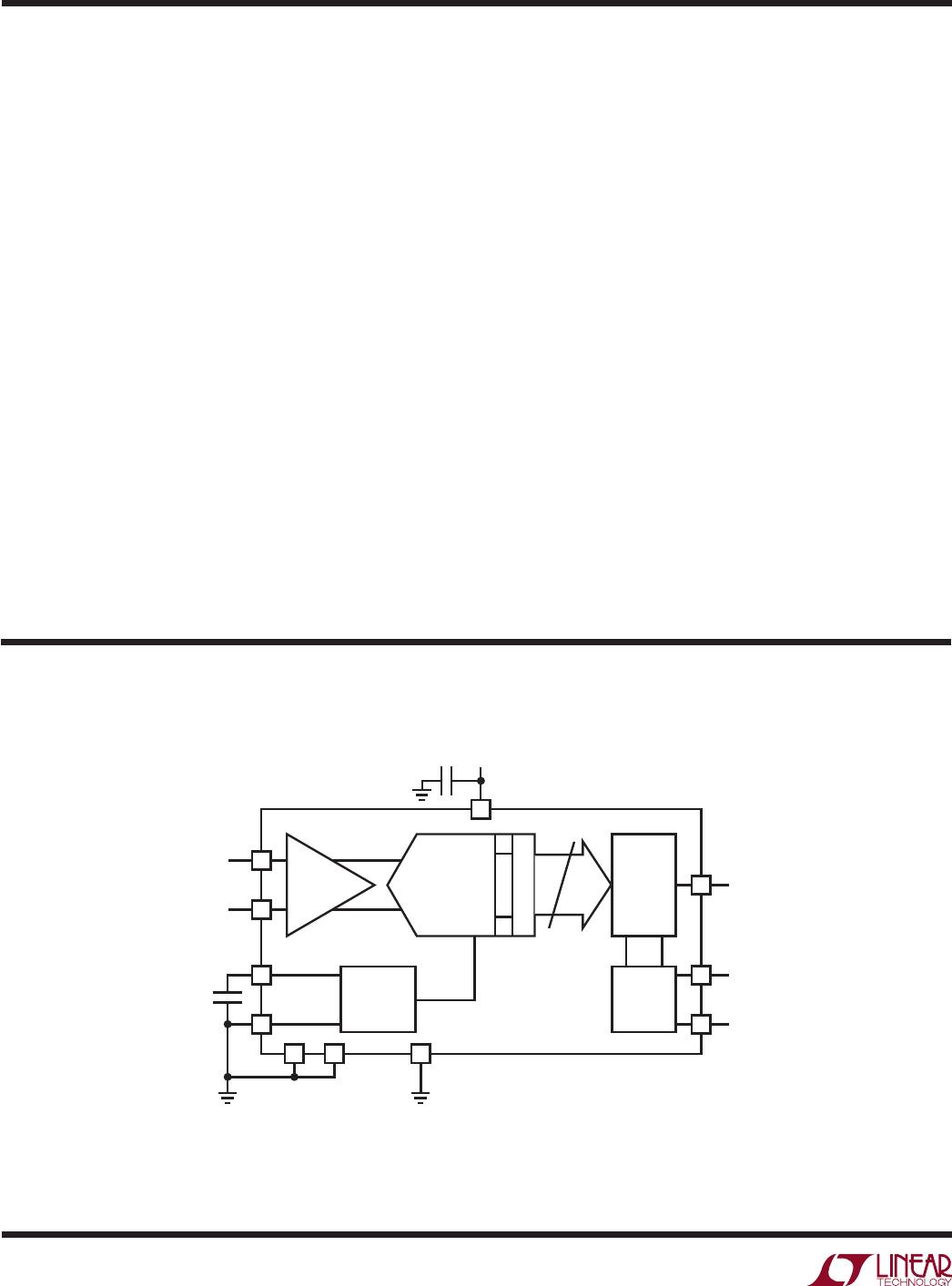
Block Diagram
pin Functions
A
IN
+
(Pin 1): Noninverting Analog Input. A
IN
+
operates
fully differentially with respect to A
IN
–
with a 0V to 2.5V
differential swing and a 0V to V
DD
common mode swing.
A
IN
–
(Pin 2): Inverting Analog Input. A
IN
–
operates
fully differentially with respect to A
IN
+
with a –2.5V to 0V
differential swing and a 0V to V
DD
common mode swing.
V
REF
(Pin 3): 2.5V Internal Reference. Bypass to GND
and to a solid analog ground plane with a 10µF ceramic
capacitor (or 10µF tantalum in parallel with 0.1µF ceramic).
Can be overdriven by an external reference between 2.55V
and V
DD
.
GND (Pins 5, 6, 11): Ground and Exposed Pad. These
ground pins and the exposed pad must be tied directly to
the solid ground plane under the part. Keep in mind that
analog signal currents and digital output signal currents
flow through these pins.
V
DD
(Pin 7): 3V Positive Supply. This single power pin
supplies 3V to the entire chip. Bypass to GND and to a
solid analog ground plane with a 10µF ceramic capacitor
(or 10µF tantalum in parallel with 0.1µF ceramic). Keep in
mind that internal analog currents and digital output signal
currents flow through this pin. Care should be taken to
place the 0.1µF bypass capacitor as close to Pins 6 and
7 as possible.
SDO (Pin 8): Three-State Serial Data Output. Each of output
data words represents the difference between A
IN
+
and
A
IN
–
analog inputs at the start of the previous conversion.
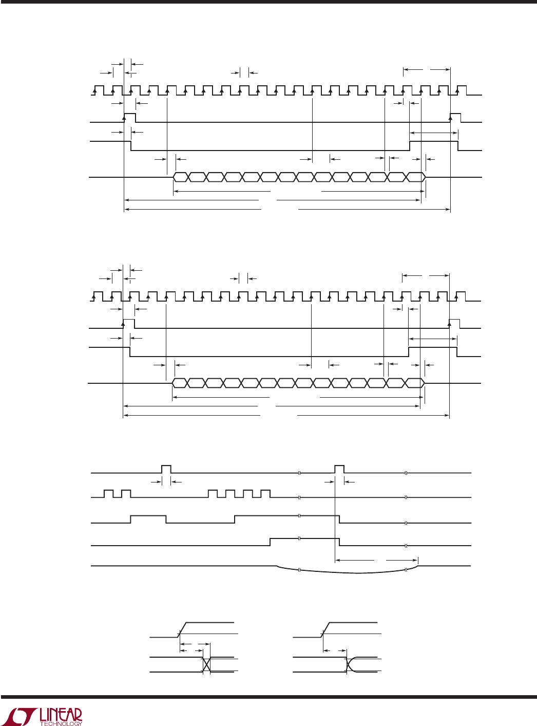
SCK (Pin 9): External Clock Input. Advances the conver-
sion process and sequences the output data on the rising
edge. Responds to T
TL (
≤3V) and 3V CMOS levels. One
or more pulses wake from sleep.
CONV (Pin 10): Convert Start. Holds the analog input signal
and starts the conversion on the rising edge. Responds
to TTL (≤3V) and 3V CMOS levels. Two pulses with SCK
in fixed high or fixed low state start Nap mode. Four or
more pulses with SCK in fixed high or fixed low state start
Sleep mode.
1403A BD
–
+
1
2
7
3
4
S & H
GND
EXPOSED PAD
LTC1403A
V
REF
10µF
A
IN
–
A
IN
+
14-BIT ADC
3V10µF
14
14-BIT LATCH
8
10
9
THREE-
STATE
SERIAL
OUTPUT
PORT
2.5V
REFERENCE
TIMING
LOGIC
V
DD
SDO
CONV
SCK
5 6 11