BGA3031 All information provided in this document is subject to legal disclaimers. © NXP Semiconductors N.V. 2014. All rights reserved.
Product data sheet Rev. 3 — 20 November 2014 10 of 23
NXP Semiconductors
BGA3031
DOCSIS 3.0 plus upstream amplifier
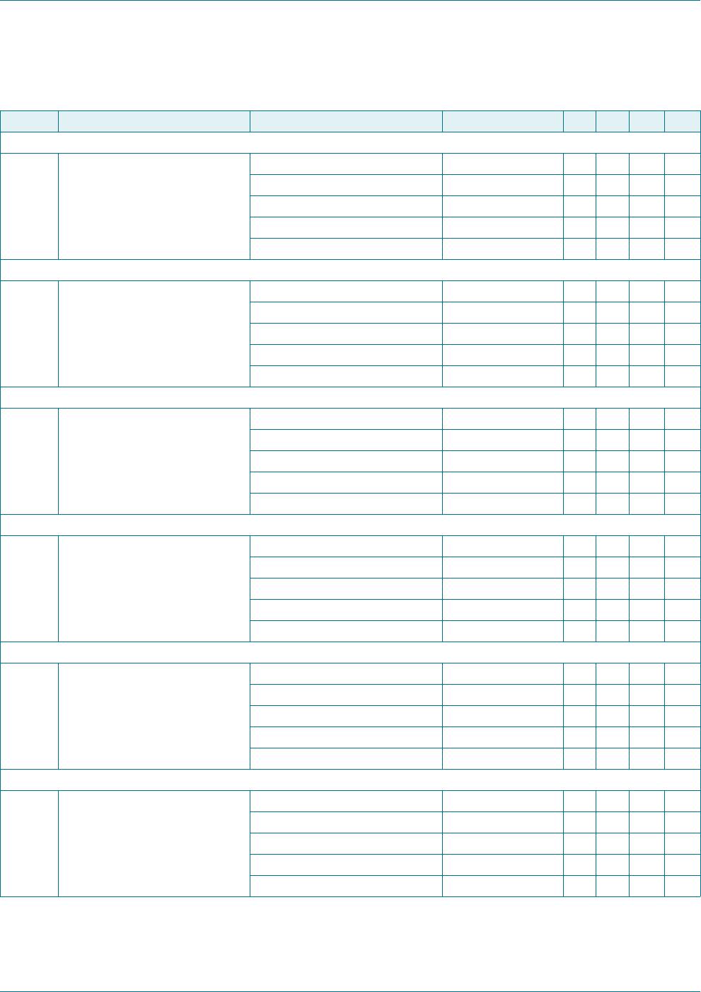
Table 13. ACLR characteristics
Typical values at V
CC
= 5 V; current setting = 3; T
amb
= 25
C; Z
i
= 200
: Z
o
= 75
; channel bandwidth = 1280 kHz;
integration bandwidth = 1280 kHz; f = 5 MHz to 85 MHz, unless otherwise specified.
Symbol Parameter Conditions DOCSIS 3.0 spec. Min Typ Max Unit
DOCSIS 3.0; 64-QAM
ACLR adjacent channel leakage ratio P
i
= 29 dBmV; P
L
= 57 dBmV
1 input channel 50 - 68 - dBc
2 input channels 47 - 62 - dBc
4 input channels 44 - 58 - dBc
8 input channels - - 56 - dBc
DOCSIS 3.0; QPSK
ACLR adjacent channel leakage ratio P
i
= 33 dBmV; P
L
= 61 dBmV
1 input channel 50 - 66 - dBc
2 input channels 47 - 58 - dBc
4 input channels 44 - 54 - dBc
8 input channels - - 52 - dBc
DOCSIS 3.0 + 3 dB; 64-QAM
ACLR adjacent channel leakage ratio P
i
= 29 dBmV; P
L
= 60 dBmV
1 input channel 50 - 68 - dBc
2 input channels 47 - 62 - dBc
4 input channels 44 - 58 - dBc
8 input channels - - 56 - dBc
DOCSIS 3.0 + 3 dB; QPSK
ACLR adjacent channel leakage ratio P
i
= 33 dBmV; P
L
= 64 dBmV
1 input channel 50 - 66 - dBc
2 input channels 47 - 58 - dBc
4 input channels 44 - 54 - dBc
8 input channels - - 48 - dBc
DOCSIS 3.0 + 4 dB; 64-QAM
ACLR adjacent channel leakage ratio P
i
= 29 dBmV; P
L
= 61 dBmV
1 input channel 50 - 68 - dBc
2 input channels 47 - 62 - dBc
4 input channels 44 - 58 - dBc
8 input channels - - 56 - dBc
DOCSIS 3.0 + 4 dB; QPSK
ACLR adjacent channel leakage ratio P
i
= 33 dBmV; P
L
= 65 dBmV
1 input channel 50 - 66 - dBc
2 input channels 47 - 58 - dBc
4 input channels 44 - 50 - dBc
8 input channels - - 42 - dBc
BGA3031 All information provided in this document is subject to legal disclaimers. © NXP Semiconductors N.V. 2014. All rights reserved.
Product data sheet Rev. 3 — 20 November 2014 11 of 23
NXP Semiconductors
BGA3031
DOCSIS 3.0 plus upstream amplifier
13. Application information
13.1 External components
Matching the balanced output of the chip to a single-ended 75 load is accomplished
using a 1 : 1 ratio transformer. For measurements in a 50 system R7 and R8 are added
for impedance transformation from 75 to 50 . R7 and R8 are not required in the final
application.
The transformer also cancels even mode distortion products and common mode signals,
such as the voltage transients that occur while enabling and disabling the amplifiers.
External capacitors are needed for the functionality of the circuit, the pins are internal
nodes in the output amplifier.
Fig 4. External components
DDD
9
&&
9
&&
9
&&
9
&&
9
&&
;
7
5)B,1
ȍ
5)B287
ȍ
ȍ
5
;
5
&
&
;
5
&
&
5
&
5
55
5

   





QF
287B1
QF
287B3
QF
*1'
QF
,1B1
,1B3
*1'
&/. '$7$ &6 7;B(1 9
&&
QF QF QF
9
&&
QF
;
&
9
*1'
9
&&
7
Table 14. List of components
For application diagram, see Figure 4
.
Component Description Value Size Supplier: Part No.
C1, C2, C3, C4 capacitor 10 nF SMD 0603
C5 capacitor 100 nF SMD 0603
C6 capacitor 10 F SMD 1206
R1, R6 resistor 0 SMD 0603
R2, R3 resistor 0 SMD 0805
R4, R5 resistor 4.7 SMD 0603
BGA3031 All information provided in this document is subject to legal disclaimers. © NXP Semiconductors N.V. 2014. All rights reserved.
Product data sheet Rev. 3 — 20 November 2014 12 of 23
NXP Semiconductors
BGA3031
DOCSIS 3.0 plus upstream amplifier
13.2 Graphs
R7 resistor 43.3 SMD 0603
R8 resistor 86.6 SMD 0603
T1 input balun - - TOKO: #617DB-1714
T2 output balun - - M/A-COM: MABA-009572-CF18A0
X1 2-pin header - -
X2, X3 SMA connector - -
X4 10-pin header - - FCI: Minitek
Table 14. List of components
…continued
For application diagram, see Figure 4.
Component Description Value Size Supplier: Part No.
V
CC
= 5 V; current setting = 3; T
amb
= 25 C;
P
i
=30dBmV.
(1) f = 5 MHz
(2) f = 42 MHz
(3) f = 85 MHz
V
CC
= 5 V; current setting = 3; T
amb
= 25 C;
P
i
=30dBmV.
(1) gain setting = 5
(2) gain setting = 20
(3) gain setting = 36
(4) gain setting = 50
(5) gain setting = 63
Fig 5. Voltage gain as a function of gain setting;
typical values
Fig 6. Voltage gain as a function of frequency;
typical values
DDD
      




JDLQVHWWLQJ
*
Y
*
Y
G%G%G%



DDD
    




I0+]
*
Y
*
Y
G%G%G%






BGA3031J

Mfr. #:
Manufacturer:
NXP Semiconductors
Description:
RF Amplifier BGA3031/HVQFN20///REEL 13 Q1 NDP
Lifecycle:
New from this manufacturer.
Delivery:
DHL FedEx Ups TNT EMS
Payment:
T/T Paypal Visa MoneyGram Western Union

Products related to this Datasheet