BGA3031 All information provided in this document is subject to legal disclaimers. © NXP Semiconductors N.V. 2014. All rights reserved.
Product data sheet Rev. 3 — 20 November 2014 7 of 23
NXP Semiconductors
BGA3031
DOCSIS 3.0 plus upstream amplifier
8.3 Tx enable / Tx disable
The amplifier can be disabled or enabled by making TX_EN (pin 9) LOW or HIGH. A LOW
to HIGH Tx enable transition will activate new programed settings. If no new settings are
programmed the last programmed setting will be re-activated.
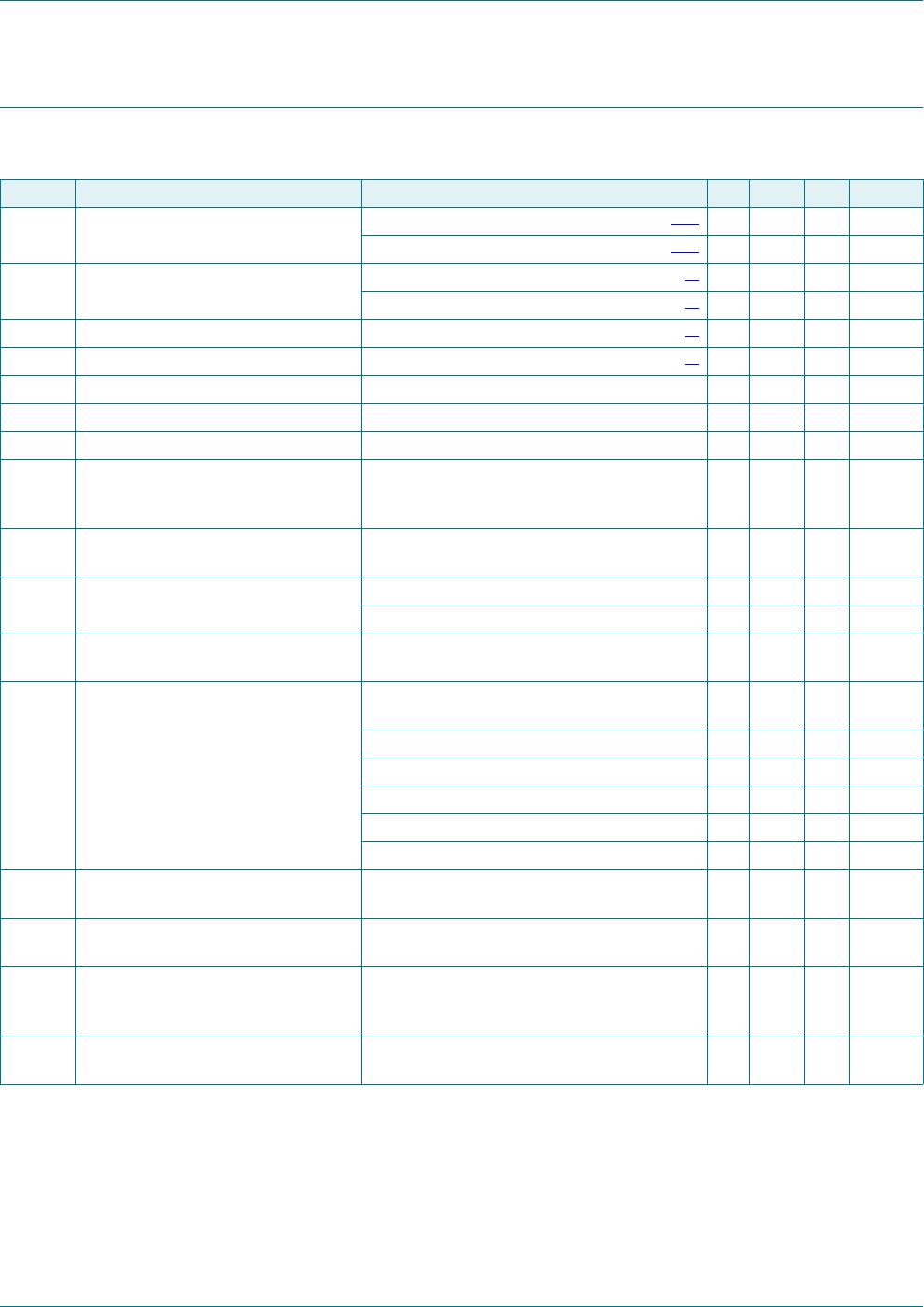
9. Limiting values
[1] All digital pins may not exceed V
CC
as the internal ESD circuit can be damaged. To prevent this it is recommended that control pins are
limited to a maximum of 5 mA.
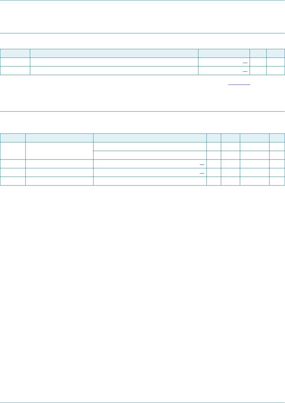
Table 8. Supply current versus gain setting
Gain setting G[5:0] Typical current (mA)
binary
notation
decimal
notation
Current setting C[1:0] Current setting C[1:0] Current setting C[1:0] Current setting C[1:0]
00 (decimal = 0) 01 (decimal = 1) 10 (decimal = 2) 11 (decimal =3)
111111 63 215 260 290 325
110111 55 215 260 290 325
110110 54 165 190 200 215
110001 49 165 190 200 215
110000 48 135 150 160 160
101000 40 135 150 160 160
100111 39 120 125 125 125
000101 5 120 125 125 125
Table 9. Limiting values
In accordance with the Absolute Maximum Rating System (IEC 60134).
Absolute Maximum Ratings are given as Limiting Values of stress conditions during operation, that must not be exceeded
under the worst probable conditions.
Symbol Parameter Conditions Min Max Unit
V
CC
supply voltage -6.0V
V
I
input voltage on pin IN_P 0.5 +6.0 V
on pin IN_N 0.5 +6.0 V
on pin CLK
[1]
0.5 +6.0 V
on pin DATA
[1]
0.5 +6.0 V
on pin CS
[1]
0.5 +6.0 V
on pin TX_EN
[1]
0.5 +6.0 V
on pin OUT_N 0.5 +6.0 V
on pin OUT_P 0.5 +6.0 V
P
i(max)
maximum input power - 40 dBmV
T
amb
ambient temperature 40 +85 C
T
stg
storage temperature 65 +150 C
T
j
junction temperature - 150 C
V
ESD
electrostatic discharge voltage Human Body Model (HBM);
According JEDEC standard 22-A114E
-4000V
Charged Device Model (CDM);
According JEDEC standard 22-C101B
-2000V