SSL21081T All information provided in this document is subject to legal disclaimers. © NXP B.V. 2013. All rights reserved.
Product data sheet Rev. 6 — 3 October 2013 10 of 22
NXP Semiconductors
SSL21081T
Compact non-dimmable LED driver IC
8.4 VCC supply
The SSL21081T is supplied using three methods:
• Under normal operation, the voltage swing on the DVDT pin is rectified within the IC
providing current towards the VCC pin
• At start-up, there is an internal current source connected to the HV pin. The current
source provides internal power until either the dV/dt supply or an external current on
the VCC pin provides the supply
• Using an auxiliary winding, the voltage can be rectified and connected to the VCC pin
via a series resistor.
The IC starts up when the voltage at the VCC pin
exceeds V
CC(startup)
. The IC locks out
(stops switching) when the voltage at the VCC pin is < V
CC(stop)
. The hysteresis between
the start and stop levels allows the IC to be supplied by a buffer capacitor until the dV/dt
supply is settled. The SSL21081T has an internal V
CC
clamp, which is an internal active
Zener (or shunt regulator). This internal active Zener limits the voltage on the supply VCC
pin to the maximum value of V
CC
. If the maximum current of the dV/dt supply minus the
current consumption of the IC (determined by the load on the gate drivers), is lower than
the maximum value of I
DD
no external Zener diode is required in the dV/dt supply circuit.
8.5 DVDT pin supply (dV/dt)
The DVDT pin is connected to an internal single-sided rectification stage. When a different
voltage with sufficient amplitude is supplied to the pin, the IC can be powered without any
other external power connection. This provides an effective method to prevent additional
high power losses, which are the result if a regulator were used for continuously powering
the IC. Unlike an auxiliary supply, additional inductor windings are not required.
8.6 VCC regulator
During supply dips, the input voltage can drop so much that it can no longer supply the
required IC current through the DVDT pin. Under these conditions, if the VCC voltage
drops to below V
CC(swon)reg
level, another regulator with a current capability of up to
I
sup(high)HV
is started. The job of the regulator is to fill in the required supply current, which
the dV/dt supply does not deliver, thus preventing that the IC enters UVLO. When the
VCC voltage exceeds the V
CC(swon)reg
level, the regulator is turned off.
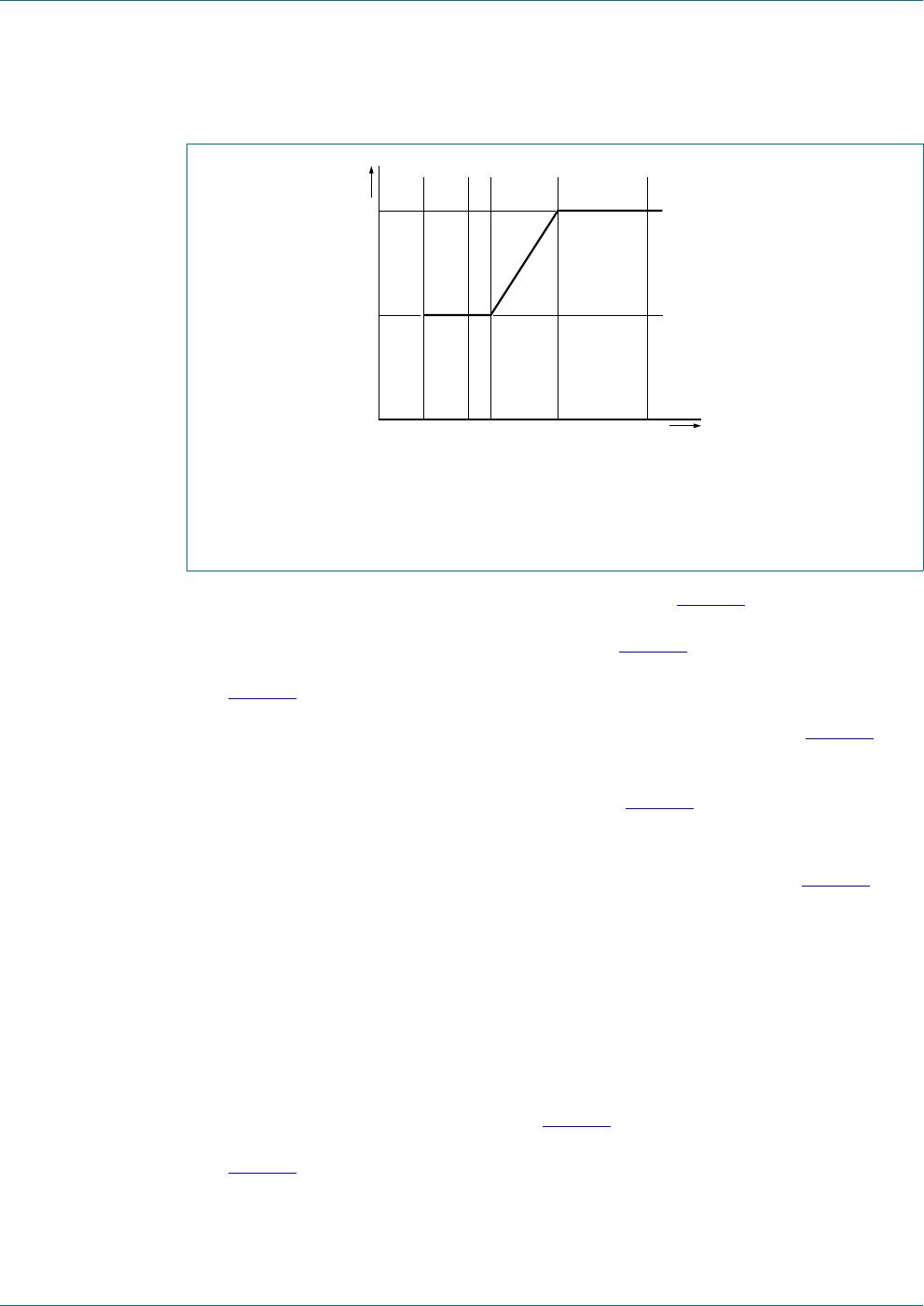
8.7 NTC functionality and PWM regulation
The NTC pin can be used as a control method for LED thermal protection. Alternatively,
the pin can be used as an input to disable/enable light output using a digital signal (PWM
regulation). The pin has an internal current source that generates the current of I
offset(NTC)
.
An NTC resistor to monitor the LED temperature can be connected directly to the NTC
pin. Depending on the resistance value and the corresponding voltage on the NTC pin,
the converter reacts as shown in Figure
6.
During start-up, before V
CC
reaches V
CC(startup)
the voltage on the NTC pin must be less
than the minimum value of V
act(tmr)NTC
. This is valid when the voltage on the NTC pin is
derived from the V
CC
using a resistive divider and a PTC in series with the resistor
between pins VCC and NTC.