13
COMMERCIAL AND INDUSTRIAL TEMPERATURE RANGES
IDT72V295/72V2105 3.3V HIGH DENSITY CMOS
SUPERSYNC FIFO
TM
131,072 x 18, 262,144 x 18
When WEN is HIGH, no new data is written in the RAM array on each
WCLK cycle.
To prevent data overflow in the IDT Standard mode, FF will go LOW,
inhibiting further write operations. Upon the completion of a valid read cycle,
FF will go HIGH allowing a write to occur. The FF is updated by two WCLK
cycles + tSKEW after the RCLK cycle.
To prevent data overflow in the FWFT mode, IR will go HIGH, inhibiting
further write operations. Upon the completion of a valid read cycle, IR will
go LOW allowing a write to occur. The IR flag is updated by two WCLK
cycles + t
SKEW after the valid RCLK cycle.
WEN is ignored when the FIFO is full in either FWFT or IDT Standard
mode.
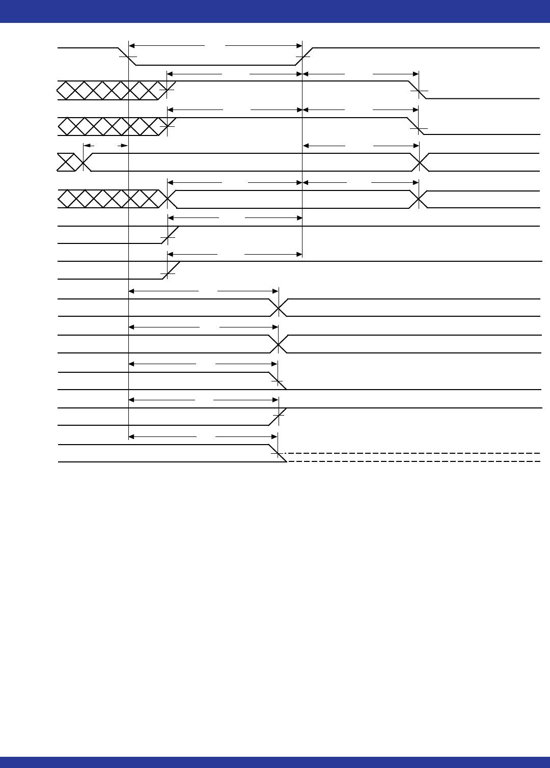
READ CLOCK ( RCLK )
A read cycle is initiated on the rising edge of the RCLK input. Data can
be read on the outputs, on the rising edge of the RCLK input. It is permissible
to stop the RCLK. Note that while RCLK is idle, the EF/OR, PAE and HF flags
will not be updated. (Note that RCLK is only capable of updating the HF flag
to HIGH.) The Write and Read Clocks can be independent or coincident.
READ ENABLE (
REN
)
When Read Enable is LOW, data is loaded from the RAM array into the
output register on the rising edge of every RCLK cycle if the device is not
empty.
When the
REN
input is HIGH, the output register holds the previous data
and no new data is loaded into the output register. The data outputs Q
0
-Q
n
maintain the previous data value.
In the IDT Standard mode, every word accessed at Qn, including the first
word written to an empty FIFO, must be requested using REN. When the
last word has been read from the FIFO, the Empty Flag (EF) will go LOW,
inhibiting further read operations. REN is ignored when the FIFO is empty.
Once a write is performed, EF will go HIGH allowing a read to occur. The
EF flag is updated by two RCLK cycles + tSKEW after the valid WCLK cycle.
In the FWFT mode, the first word written to an empty FIFO automatically
goes to the outputs Qn, on the third valid LOW to HIGH transition of RCLK
+ tSKEW after the first write. REN does not need to be asserted LOW. In
order to access all other words, a read must be executed using REN. The
RCLK LOW to HIGH transition after the last word has been read from the
FIFO, Output Ready (OR) will go HIGH with a true read (RCLK with REN =
LOW), inhibiting further read operations. REN is ignored when the FIFO is
empty.
SERIAL ENABLE ( SEN )
The SEN input is an enable used only for serial programming of the
offset registers. The serial programming method must be selected during
Master Reset. SEN is always used in conjunction with LD. When these lines
are both LOW, data at the SI input can be loaded into the program register
one bit for each LOW-to-HIGH transition of WCLK. (See Figure 4.)
When SEN is HIGH, the programmable registers retains the previous
settings and no offsets are loaded. SEN functions the same way in both IDT
Standard and FWFT modes.
OUTPUT ENABLE ( OE )
When Output Enable is enabled (LOW), the parallel output buffers receive
data from the output register. When OE is HIGH, the output data bus (Q
n
) goes
into a high impedance state.
LOAD ( LD )
This is a dual purpose pin. During Master Reset, the state of the LD input
determines one of two default offset values (127 or 1,023) for the PAE and PAF
flags, along with the method by which these offset registers can be pro-
grammed, parallel or serial. After Master Reset, LD enables write operations
to and read operations from the offset registers. Only the offset loading method
currently selected can be used to write to the registers. Offset registers can be
read only in parallel. A LOW on LD during Master Reset selects a default PAE
offset value of 07FH (a threshold 127 words from the empty boundary), a default
PAF offset value of 07FH (a threshold 127 words from the full boundary), and
parallel loading of other offset values. A HIGH on LD during Master Reset
selects a default PAE offset value of 3FFH (a threshold 1,023 words from the
empty boundary), a default PAF offset value of 3FFH (a threshold 1,023 words
from the full boundary), and serial loading of other offset values.
After Master Reset, the LD pin is used to activate the programming
process of the flag offset values PAE and PAF. Pulling LD LOW will begin a
serial loading or parallel load or read of these offset values. See Figure 4,
Programmable Flag Offset Programming Sequence.
OUTPUTS:
FULL FLAG ( FF/IR )
This is a dual purpose pin. In IDT Standard mode, the Full Flag (FF) function
is selected. When the FIFO is full, FF will go LOW, inhibiting further write
operations. When FF is HIGH, the FIFO is not full. If no reads are performed
after a reset (either
MRS
or PRS), FF will go LOW after D writes to the FIFO
(D = 131,072 for the IDT72V295 and 262,144 for the IDT72V2105
). See Figure
7, Write Cycle and Full Flag Timing (IDT Standard Mode), for the relevant
timing information.
In FWFT mode, the Input Ready (IR) function is selected. IR goes LOW
when memory space is available for writing in data. When there is no longer
any free space left, IR goes HIGH, inhibiting further write operations. If no
reads are performed after a reset (either MRS or PRS), IR will go HIGH after
D writes to the FIFO (D = 131,073 for the IDT72V295 and 262,145 for the
IDT72V2105) See Figure 9, Write Timing (FWFT Mode), for the relevant
timing information.
The IR status not only measures the contents of the FIFO memory, but
also counts the presence of a word in the output register. Thus, in FWFT
mode, the total number of writes necessary to deassert IR is one greater
than needed to assert FF in IDT Standard mode.
FF/IR is synchronous and updated on the rising edge of WCLK.
FF/IR are
double register-buffered outputs.
EMPTY FLAG ( EF/OR )
This is a dual purpose pin. In the IDT Standard mode, the Empty Flag
(EF) function is selected. When the FIFO is empty, EF will go LOW, inhibiting
further read operations. When EF is HIGH, the FIFO is not empty. See
Figure 8, Read Cycle, Empty Flag and First Word Latency Timing (IDT
Standard Mode), for the relevant timing information.
In FWFT mode, the Output Ready (OR) function is selected. OR goes
LOW at the same time that the first word written to an empty FIFO appears
valid on the outputs. OR stays LOW after the RCLK LOW to HIGH transition
that shifts the last word from the FIFO memory to the outputs. OR goes
HIGH only with a true read (RCLK with REN = LOW). The previous data
stays at the outputs, indicating the last word was read. Further data reads
are inhibited until OR goes LOW again.
See Figure 10, Read Timing (FWFT
Mode), for the relevant timing information.