22
COMMERCIAL AND INDUSTRIAL TEMPERATURE RANGES
IDT72V295/72V2105 3.3V HIGH DENSITY CMOS
SUPERSYNC FIFO
TM
131,072 x 18, 262,144 x 18
NOTES:
1. m = PAF offset .
2. D = maximum FIFO depth.
In IDT Standard mode: D = 131,072 for the IDT72V295 and 262,144 for the IDT72V2105.
In FWFT mode: D = 131,073 for the IDT72V295 and 262,145 for the IDT72V2105.
3.
t
SKEW2
is the minimum time between a rising RCLK edge and a rising WCLK edge to guarantee that PAF will go HIGH (after one WCLK cycle plus t
PAF
). If the time between the rising edge of
RCLK and the rising edge of WCLK is less than t
SKEW2
, then the PAF deassertion time may be delayed one extra WCLK cycle.
4. PAF is asserted and updated on the rising edge of WCLK only.
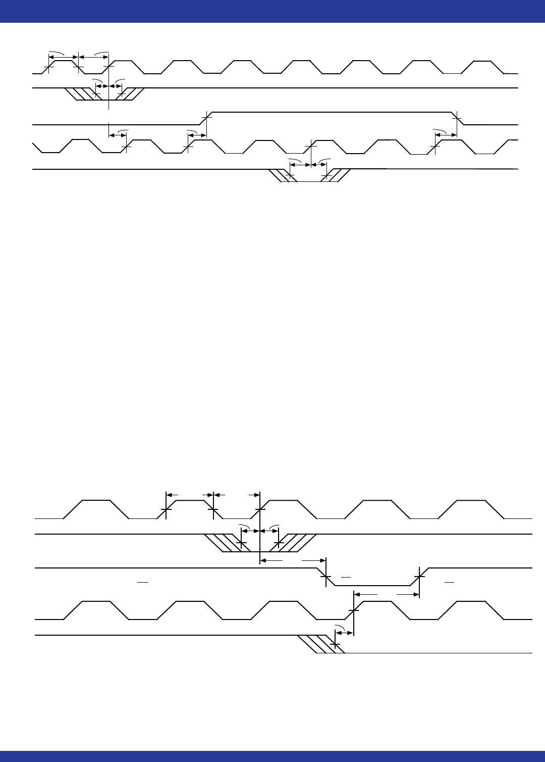
Figure 16. Programmable Almost-Full Flag Timing (IDT Standard and FWFT Modes)
NOTE:
1. OE = LOW
Figure 15. Parallel Read of Programmable Flag Registers (IDT Standard and FWFT Modes)
Figure 14. Parallel Loading of Programmable Flag Registers (IDT Standard and FWFT Modes)
WCLK
t
ENH
t
CLKH
t
CLKL
WEN
PAF
RCLK
t
PAF
REN
4668 drw 19
t
ENS
t
ENH
t
ENS
D - (m+1) words in FIFO
(2)
t
PAF
D - m words in FIFO
(2)
t
SKEW2
(3)
1
2
12
D-(m+1) words
in FIFO
(2)
4668 drw 17
WCLK
LD
WEN
D
0
- D
15
t
LDS
t
ENS
PAE OFFSET
(
LSB
)
t
DS
t
DH
t
ENH
PAF OFFSET
(
LSB
)
PAF OFFSET
(
MSB
)
t
LDH
t
CLK
t
DH
t
CLKH
t
CLKL
t
ENH
PAE OFFSET
(
MSB
)
t
LDH
4668 drw 18
RCLK
LD
REN
Q
0
- Q
15
t
LDH
t
LDS
t
ENS
DATA IN OUTPUT REGISTER
t
ENH
t
ENH
t
LDH
t
CLK
t
A
t
A
t
CLKH
t
CLKL
PAF OFFSET
(MSB)
PAF OFFSET
(LSB)
PAE OFFSET
(MSB)
PAE OFFSET
(LSB)
23
COMMERCIAL AND INDUSTRIAL TEMPERATURE RANGES
IDT72V295/72V2105 3.3V HIGH DENSITY CMOS
SUPERSYNC FIFO
TM
131,072 x 18, 262,144 x 18
NOTES:
1. For IDT Standard mode: D = maximum FIFO depth. D = 131,072 for the IDT72V295 and 262,144 for the IDT72V2105.
2. For FWFT mode: D = maximum FIFO depth. D = 131,073 for the IDT72V295 and 262,145 for the IDT72V2105.
NOTES:
1. n = PAE offset.
2. For IDT Standard mode
3. For FWFT mode.
4.
tSKEW2 is the minimum time between a rising WCLK edge and a rising RCLK edge to guarantee that PAE will go HIGH (after one RCLK cycle plus tPAE). If the time between the rising edge of
WCLK and the rising edge of RCLK is less than tSKEW2, then the PAE deassertion may be delayed one extra RCLK cycle.
5. PAE is asserted and updated on the rising edge of WCLK only.
Figure 18. Half-Full Flag Timing (IDT Standard and FWFT Modes)
Figure 17. Programmable Almost-Empty Flag Timing (IDT Standard and FWFT Modes)
WCLK
t
ENH
t
CLKH
t
CLKL
WEN
PAE
RCLK
t
ENS
n words in FIFO
(2)
,
n+1 words in FIFO
(3)
t
PAE
t
SKEW2
(4)
t
PAE
12 12
REN
4668 drw 20
t
ENS
t
ENH
n+1 words in FIFO
(2)
,
n+2 words in FIFO
(3)
n words in FIFO
(2)
,
n+1 words in FIFO
(3)
WCLK
tENS
tENH
WEN
HF
tENS
tHF
RCLK
tHF
REN
4668 drw 21
tCLKLtCLKH
D/2 words in FIFO
(1)
,
[
+ 1
]
words in FIFO
(2)
D -1
2
D/2 + 1 words in FIFO
(1)
,
[
+ 2
]
words in FIFO
(2)
D-1
2
D/2 words in FIFO
(1)
,
[
+ 1
]
words in FIFO
(2)
D-1
2
24
COMMERCIAL AND INDUSTRIAL TEMPERATURE RANGES
IDT72V295/72V2105 3.3V HIGH DENSITY CMOS
SUPERSYNC FIFO
TM
131,072 x 18, 262,144 x 18
NOTES:
1. Use an AND gate in IDT Standard mode, an OR gate in FWFT mode.
2. Do not connect any output control signals directly together.
3. FIFO #1 and FIFO #2 must be the same depth, but may be different word widths.
OPTIONAL CONFIGURATIONS
WIDTH EXPANSION CONFIGURATION
Word width may be increased simply by connecting together the control
signals of multiple devices. Status flags can be detected from any one
device. The exceptions are the EF and FF functions in IDT Standard mode
and the IR and OR functions in FWFT mode. Because of variations in skew
between RCLK and WCLK, it is possible for EF/FF deassertion and IR/OR
assertion to vary by one cycle between FIFOs. In IDT Standard mode, such
Figure 19. Block Diagram of 131,072 x 36 and 262,144 x 36 Width Expansion
problems can be avoided by creating composite flags, that is, ANDing EF
of every FIFO, and separately ANDing FF of every FIFO. In FWFT mode,
composite flags can be created by ORing OR of every FIFO, and separately
ORing IR of every FIFO.
Figure 23 demonstrates a width expansion using two IDT72V295/
72V2105 devices. D0-D17 from each device form a 36-bit wide input bus
and Q0-Q17 from each device form a 36-bit wide output bus. Any word width
can be attained by adding additional IDT72V295/72V2105 devices.
WRITE CLOCK (WCLK)
m + n
mn
MASTER RESET (MRS)
READ CLOCK (RCLK)
DATA OUT
nm + n
WRITE ENABLE (WEN)
FULL FLAG/INPUT READY (FF/IR) #1
PROGRAMMABLE (PAF)
PROGRAMMABLE (PAE)
E
MPTY FLAG/OUTPUT READY (EF/OR)
#2
OUTPUT ENABLE (OE)
READ ENABLE (REN)
m
LOAD (LD)
IDT
72V295
72V2105
EMPTY FLAG/OUTPUT READY (EF/OR)
#1
PARTIAL RESET (PRS)
IDT
72V295
72V2105
4668 drw 22
FULL FLAG/INPUT READY (FF/IR) #2
HALF-FULL FLAG (HF)
FIRST WORD FALL THROUGH/
SERIAL INPUT (FWFT/SI)
RETRANSMIT (RT)
FIFO
#2
GATE
(1)
GATE
(1)
D0
-
Dm
DATA IN
Dm
+1 - Dn
Q
0
-
Qm
Qm
+1 - Qn
FIFO
#1

72V295L10PFG

Mfr. #:
Manufacturer:
IDT
Description:
FIFO 3.3V 4M SUPER SYNC II
Lifecycle:
New from this manufacturer.
Delivery:
DHL FedEx Ups TNT EMS
Payment:
T/T Paypal Visa MoneyGram Western Union