1©2016 Integrated Device Technology, Inc Revision C January 27, 2016
LOCK_DET
DATA_OUT
nDATA_OUT
CLK_OUT
nCLK_OUT
STS12
nCAP
CAP
BYPASS
DATA_IN
nDATA_IN
SD
LOCK_REFN
REF_CLK
PLL
0
1
Pullup/Pulldown
Pulldown
Pulldown
Pulldown
Pulldown
Pulldown
Pullup
General Description
The 894D115I-04 is a clock and data recovery circuit. The device
is designed to extract the clock signal from a NRZ-coded STM-4
(OC-12/STS-12) or STM-1 (OC-3/STS-3) input data signal. The
output signals of the device are the recovered clock and retimed
data signals. Input and output are differential signals for best
signal integrity and to support high clock and data rates. All control
inputs and outputs are single-ended signals. An internal PLL is
used for clock generation and recovery. An external clock input is
provided to establish an initial operating frequency of the clock
recovery PLL and to provide a clock reference in the absence of
serial input data. The device supports a signal detect input and a
lock detect output. A bypass circuit is provided to facilitate factory
tests.
Features
Clock recovery for STM-4 (OC-12/STS-12) and
STM-1 (OC-3/STS-3)
Input: NRZ data (622.08 or 155.52 Mbit/s)
Output: clock signal (622.08MHz or 155.52MHz) and retimed
data signal at 622.08 or 155.52 Mbit/s
Internal PLL for clock generation and clock recovery
Differential inputs can accept LVPECL levels
Differential LVDS data and clock outputs
Lock reference input and PLL lock output
19.44MHz reference clock input
Full 3.3V supply mode
-40°C to 85°C operating temperature
Available in lead-free (RoHS 6) package
See 894D115I for a clock/data recovery circuit with a TSSOP
EPAD package and LVPECL outputs
See 894D115I-01 for a clock/data recovery circuit with LVPECL
outputs
Block Diagram
Pin Assignment
894D115I-04
20-Lead TSSOP
6.5mm x 4.4mm x 0.925mm
package body
G Package
Top View
1
2
3
4
5
6
7
8
9
10
20
19
18
17
16
15
14
13
12
11
GND
LOCK_REFN
REF_CLK
STS12
LOCK_DET
GND_PLL
nDATA_IN
DATA_IN
V
DDA
V
DD
VDDA
GND_PLL
CAP
nCAP
BYPASS
SD
DATA_OUT
nDATA_OUT
CLK_OUT
nCLK_OUT
894D115I-04
Data Sheet
OC-12/STM-4 AND OC-3/STM-1
Clock/Data Recovery Device
2©2016 Integrated Device Technology, Inc Revision C January 27, 2016
894D115I-04 Data Sheet
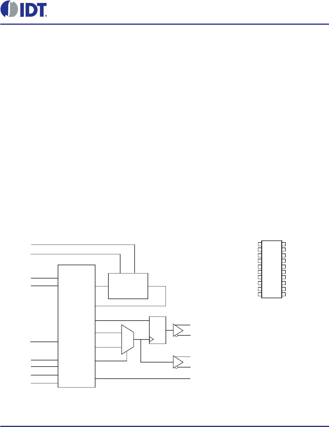
Functional Description
The 894D115I-04 is designed to extract the clock from a
NRZ-coded STM-4 (OC-12/STS-12) or STM-1 (OC-3/STS-3) input
data signals. The output signals are the recovered clock and
retimed data signals. The device contains an integrated PLL for
clock generation and to lock the output clock to the input data
stream. The PLL attempts to lock to the reference clock input
(REF_CLK) in absence of the serial data stream or if it is forced to
by the control inputs LOCK_REFN or SD. The output clock
frequency is controlled by the STS12 input. The output frequency
is 622.08MHz in STM-4/OC-12/STS-12 mode and 155.52MHz in
STM-1/OC-3/STS-3 mode.
The 894D115I-04 will maintain an output (CLK_OUT/ nCLK_OUT)
frequency deviation of less than ±500ppm with respect to the
REF_CLK reference frequency in a loss of signal state (LOS).
During the LOS state, the data outputs (DATA_OUT/
nDATA_OUT) are held at logic low state. An LOS state of the
894D115I-04 is given when BYPASS is set to the logic low state
and either one of the SD or LOCK_REFN inputs are at a logic low
state.
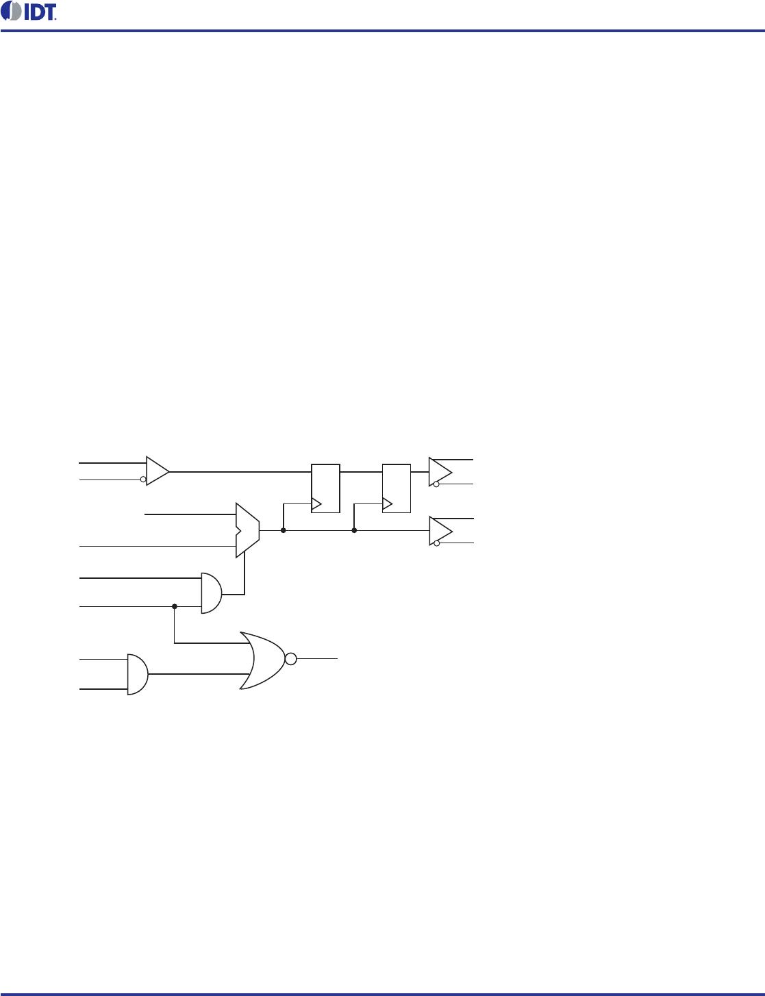
This will enable the use of the SD (signal detect) and the
LOCK_REFN (lock-to-reference) inputs to accept loss of signal
status information from electro-optical receivers. Please refer to
Figure 1, “Signal Detect/PLL Bypass Operation Control Diagram”,
for details.
The lock detect output (LOCK_DET) can be used to monitor the
operating state of the clock/data recovery circuit. LOCK_DET is
set to logic low level when the internal oscillator of the PLL and
the reference clock (REF_CLK) deviate from each other by more
than 500ppm, or when the CDR is forced to lock the REF_CLK
input by the LOCK_REFN or SD control input. LOCK_DET is set
to high when the PLL is locked to the input data stream and
indicates valid clock and data output signals.
The BYPASS pin should be set to logic low state in all
applications. BYPASS set to logic high state is used during factory
test. In BYPASS mode (BYPASS and STS12 are at logic high
state), the internal PLL is bypassed and the inverted REF_CLK
input signal is output at CLK_OUT/nCLK_OUT.
Figure 1. Signal Detect/PLL BYPASS Operation Control Diagram
LOS
(on-chip)
DATA_OUT
nDATA_OUT
CLK_OUT
nCLK_OUT
STS12
BYPASS
DATA_IN
nDATA_IN
PLL Clock
(on-chip)
SD
LOCK_REFN
REF_CLK
0
1
Pullup/Pulldown
Pulldown
Pulldown
Pulldown
Pulldown
Pulldown
Pullup
3©2016 Integrated Device Technology, Inc Revision C January 27, 2016
894D115I-04 Data Sheet
Table 1. Signal Detect/PLL BYPASS Operation Control Table
Table 2. Pin Descriptions
NOTE: Pullup and Pulldown refer to internal input resistors. See Table 3, Pin Characteristics, for typical values.
Inputs Outputs
STS12 BYPASS LOCK_REFN SD DATA_OUT CLK_OUT
1011DATA_INPLL Clock
1010LOWPLL Clock
1001LOWPLL Clock
1000LOWPLL Clock
1 1 X X DATA_IN REF_CLK
0011DATA_INPLL Clock
0010LOWPLL Clock
0001LOWPLL Clock
0000LOWPLL Clock
0 1 X X Not Allowed Not Allowed
Number Name Type Description
1, 20 V
DDA
Power Analog supply pins.
2 DATA_IN Input Pulldown Non-inverting differential signal input.
3 nDATA_IN Input
Pullup/
Pulldown
Inverting differential signal input. V
DD
/2 default when left floating.
4, 19 GND_PLL Power Power supply ground.
5 LOCK_DT Output Lock detect output. See Table 4A. Single-ended LVPECL interface levels.
6 STS12 Input Pulldown
STM-4 (OC-12, STS-12) or STM-1 (OC-3, STS-3) selection mode. See Table 4B.
LVCMOS/LVTTL interface levels.
7 REF_CLK Input Pulldown Reference clock input of 19.44MHz. LVCMOS/LVTTL interface levels.
8 LOCK_REFN Input Pullup Lock to REF_CLK input. See Table 4C. LVCMOS/LVTTL interface levels.
9 GND Power Power supply ground.
10 V
DD
Power Core supply pin.
11,
12
nCLK_OUT,
CLK_OUT
Output Differential clock output pair. LVDS interface levels.
13,
14
nDATA_OUT,
DATA_OUT
Output Differential clock output pair. LVDS interface levels.
15 SD Input Pulldown
Signal detect input. Typically, SD is driven by the signal detect output of the
electro-optical module. See Table 4D. Single-ended LVPECL interface levels.
16 BYPASS Input Pulldown PLL bypass mode. See Table 4E. LVCMOS/LVTTL interface levels.
17, 18 nCAP, CAP Input External loop filter (1.0µF ±10%).

894D115AGI-04LF

Mfr. #:
Manufacturer:
IDT
Description:
Clock Generators & Support Products STM-1/-4 OC-3/-12 CLK/DATA RECOVERY
Lifecycle:
New from this manufacturer.
Delivery:
DHL FedEx Ups TNT EMS
Payment:
T/T Paypal Visa MoneyGram Western Union

Products related to this Datasheet