7©2016 Integrated Device Technology, Inc Revision C January 27, 2016
894D115I-04 Data Sheet
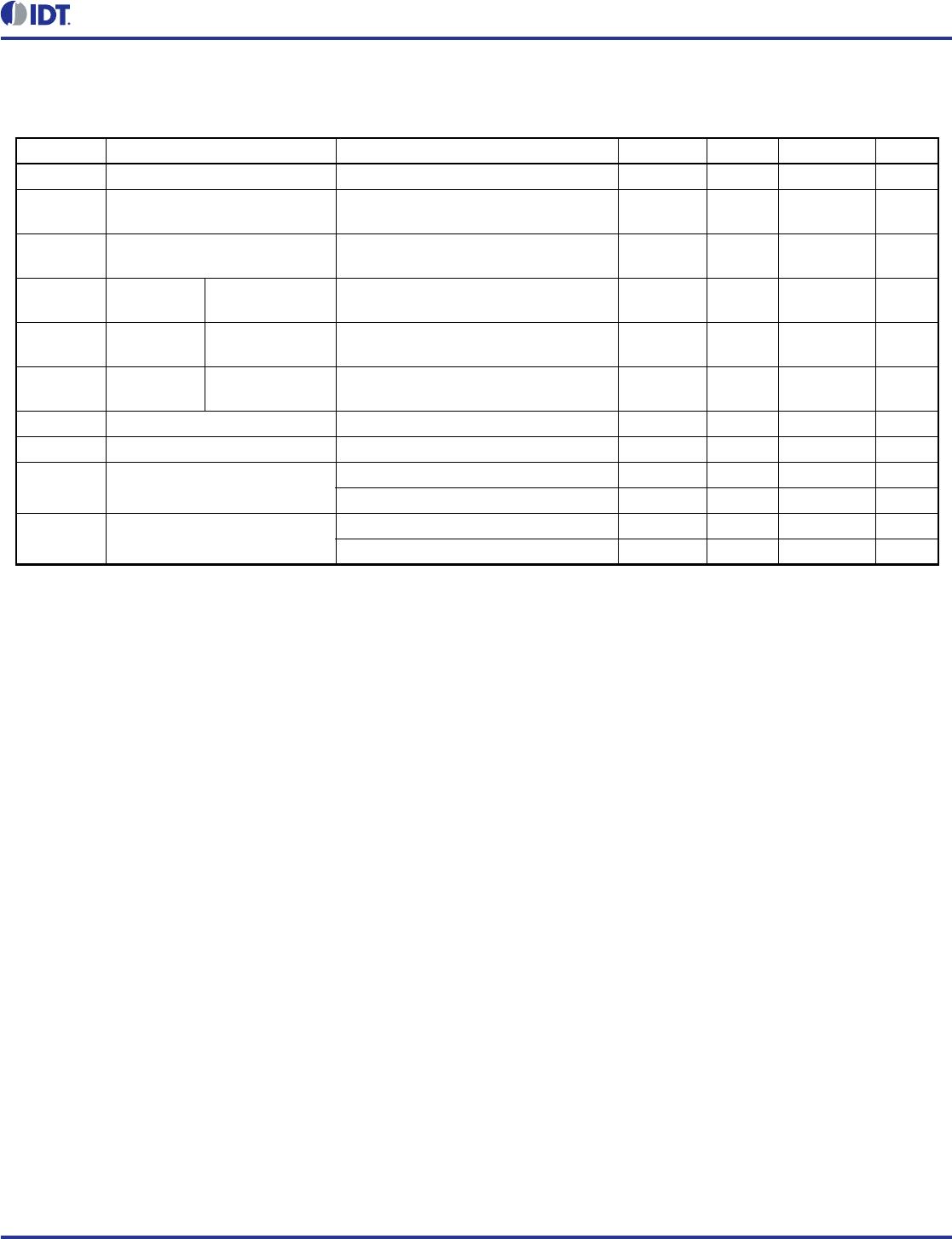
AC Electrical Characteristics
Table 6. AC Characteristics, V
DD
= 3.3V ± 5%, V
EE
= 0V, T = -40°C to 85°C
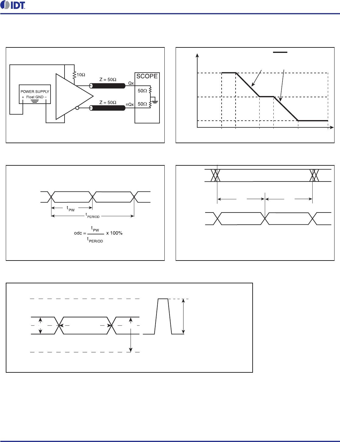
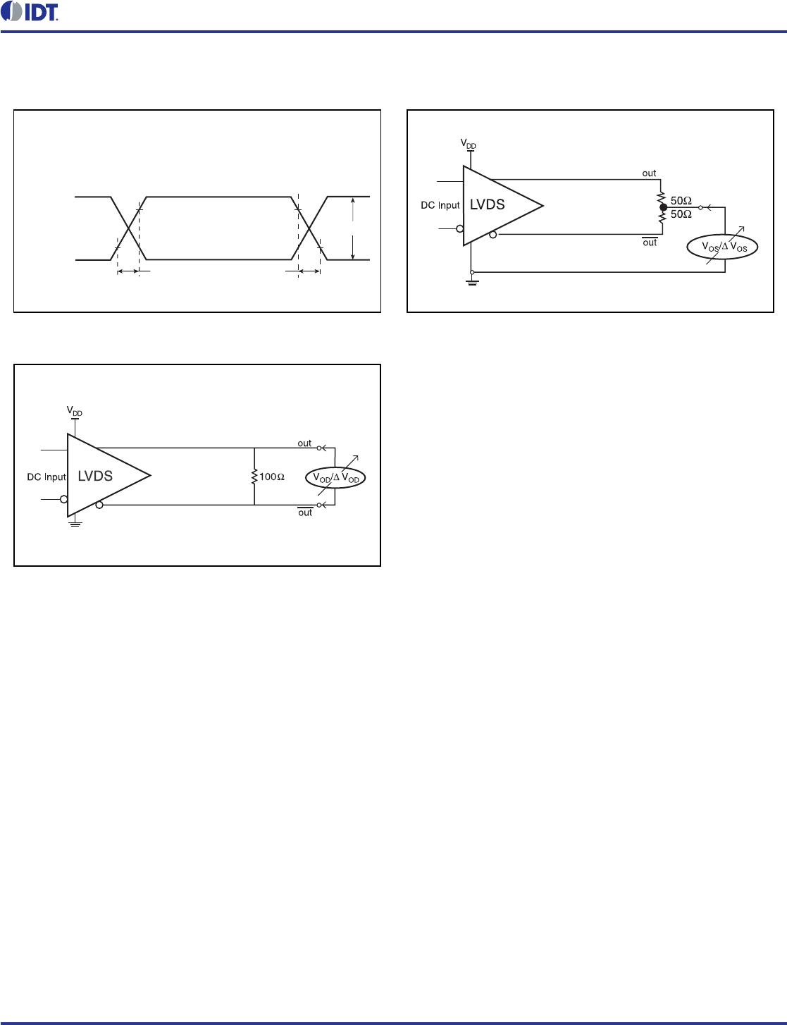
NOTE 1: See diagram in Parameter Measurement Information section.
Parameter Symbol Test Conditions Minimum Typical Maximum Units
f
VCO
VCO Center Frequency 622.08 MHz
f
TOL
CRU’s Reference Clock
Frequency Tolerance
-250 250 ppm
fT
REF_CLK
OC-12/STS-12 Capture Range
With respect to the fixed
reference frequency
±500 ppm
t
LOCK
Acquisition
Lock Time
OC-12/STS-12
Valid REF_CLK and device already
powered-up
16 µs
J
GEN_CLK
Jitter
Generation
CLK_OUT/
nCLK_OUT
14ps rms (max.) jitter on
DATA_IN/nDATA_IN
0.005 0.01 UI
J
TOL
Jitter
Tolerance
OC-12/STS-12;
NOTE 1
Sinusoidal input jitter of DATA_IN/
nDATA_IN from 250kHz to 5MHz
0.45 UI
t
R
/ t
F
Output Rise/Fall Time; NOTE 1 20% to 80% 500 ps
odc Output Duty Cycle; NOTE 1 20% minimum transition density 45 55 %
t
S
Setup Time; NOTE 1
STS-3 2000 3220 ps
STS-12 450 800 ps
t
H
Hold Time; NOTE 1
STS-3 3000 3220 ps
STS-12 650 800 ps
8©2016 Integrated Device Technology, Inc Revision C January 27, 2016
894D115I-04 Data Sheet
Parameter Measurement Information
LVDS 3.3V Output Load AC Test Circuit
Output Duty Cycle/Pulse Width/Period
Jitter Tolerance Specification
Setup/Hold Time
Differential Input Level
3.3V ±5%
V
DD
V
DDA
nCLK_OUT,
nDATA_OUT
CLK_OUT,
DATA_OUT
Requirement Mask
Input Jitter Amplitude (UIpp)
Jitter Frequency (Hz)
slope = -20dB/decade
15
1.5
0.15
10 30 300 25k 250k
5M
t
H
t
SU
The re-timed data output (DATA_OUT) can be captured with the
rising edge of the clock output signal (CLOCK_OUT).
DATA_OUT is valid the specified setup time before the rising
CLK_OUT signal and remains valid the specified hold time after
nDATA_OUT
DATA_OUT
CLK_OUT
nCLK_OUT
V
IH
Cross Points
V
PP
ΔV
IN
= DATA_IN - nDATA_IN
V
DD
nDATA_IN
DATA_IN
GND
9©2016 Integrated Device Technology, Inc Revision C January 27, 2016
894D115I-04 Data Sheet
Parameter Measurement Information, continued
Output Rise/Fall Time
Offset Voltage Setup
Differential Output Voltage Setup
20%
80%
80%
20%
t
R
t
F
V
OD
nCLK_OUT,
CLK_OUT,
nDATA_OUT
DATA_OUT

894D115AGI-04LF

Mfr. #:
Manufacturer:
IDT
Description:
Clock Generators & Support Products STM-1/-4 OC-3/-12 CLK/DATA RECOVERY
Lifecycle:
New from this manufacturer.
Delivery:
DHL FedEx Ups TNT EMS
Payment:
T/T Paypal Visa MoneyGram Western Union

Products related to this Datasheet