10©2016 Integrated Device Technology, Inc Revision C January 27, 2016
894D115I-04 Data Sheet
Application Information
Power Supply Filtering Technique
As in any high speed analog circuitry, the power supply pins are
vulnerable to random noise. To achieve optimum jitter perform-
ance, power supply isolation is required. The 894D115I-04
provides separate power supplies to isolate any high switching
noise from the outputs to the internal PLL. V
DD
and V
DDA
should
be individually connected to the power supply plane through vias,
and 0.01µF bypass capacitors should be used for each pin. Figure
2 illustrates this for a generic V
DD
pin and also shows that V
DDA
requires that an additional 10 resistor along with a 10F bypass
capacitor be connected to the V
DDA
pin.
Figure 2. Power Supply Filtering
Recommendations for Unused Input and Output Pins
Inputs:
LVCMOS Control Pins
All control pins have internal pull-ups or pull-downs; additional
resistance is not required but can be added for additional
protection. A 1k resistor can be used.
Outputs:
LVDS Outputs
All unused LVDS output pairs can be either left floating or
terminated with 100 across. If they are left floating, there should
be no trace attached.
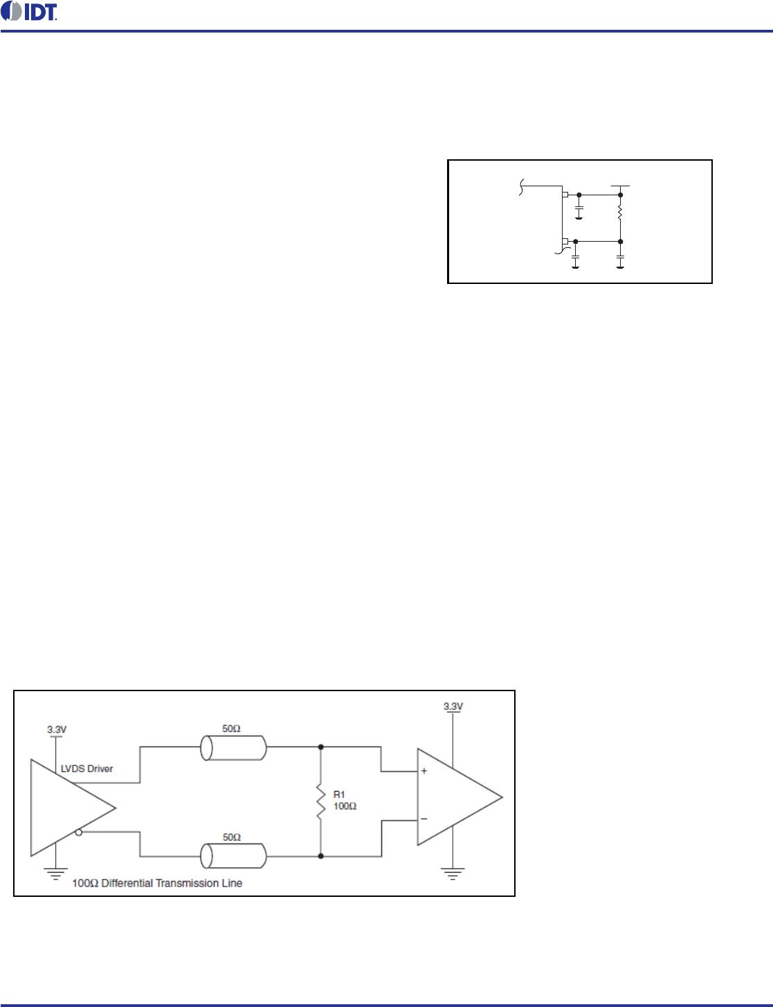
3.3V LVDS Driver Termination
A general LVDS interface is shown in Figure 3. In a 100 differ-
ential transmission line environment, LVDS drivers require a
matched load termination of 100 across near the receiver input.
Figure 3. Typical LVDS Driver Termination
V
DD
V
DDA
3.3V
10Ω
10µF.01µF
.01µF
11©2016 Integrated Device Technology, Inc Revision C January 27, 2016
894D115I-04 Data Sheet
Power Considerations
This section provides information on power dissipation and junction temperature for the 894D115I-04.
Equations and example calculations are also provided.
1. Power Dissipation.
The total power dissipation for the 894D115I-04 is the sum of the core power plus the power dissipated in the load(s).
The following is the power dissipation for V
DD
= 3.465V, which gives worst case results.
NOTE: Please refer to Section 3 for details on calculating power dissipated in the load.
Core and LVDS Output Power Dissipation
Power (core, LVDS)
MAX
= V
DD_MAX
* (I
DD_MAX
+ I
DDA_MAX
) = 3.4655V * (92mA + 10mA) = 353.43mW
Single-ended LVPECL Output Power Dissipation
Power (LVPECL outputs)
MAX
= 19.8mW (for logic high)
Total Power_
MAX
(3.465V, with all outputs switching) = 353.43mW + 19.8mW = 373.23mW
2. Temperature.
Junction temperature, Tj, is the temperature at the junction of the bond wire and bond pad and directly affects the reliability of the device.
The maximum recommended junction temperature for HiPerClockS devices is 125°C.
Lower temperature refers to ambient temperature, maximum temperature refers to case temperature.
Table 7. Thermal Resistance
JA
for 20 Lead TSSOP, Forced Convection
JA
by Velocity
Meters per Second 012.5
Multi-Layer PCB, JEDEC Standard Test Boards 81.3°C/W 76.9°C/W 74.8°C/W
12©2016 Integrated Device Technology, Inc Revision C January 27, 2016
894D115I-04 Data Sheet
Reliability Information
Table 8.
JA
vs. Air Flow Table for a 20 Lead TSSOP
Transistor Count
The transistor count for 894D115I-04 is: 10,557
Compatible with VSC8115
Package Outline and Package Dimensions
Package Outline - G Suffix for 20 Lead TSSOP Table 9. Package Dimensions
Reference Document: JEDEC Publication 95, MO-153
JA
by Velocity
Meters per Second 012.5
Multi-Layer PCB, JEDEC Standard Test Boards 81.3°C/W 76.9°C/W 74.8°C/W
All Dimensions in Millimeters
Symbol Minimum Maximum
N 20
A 1.20
A1 0.05 0.15
A2 0.80 1.05
b 0.19 0.30
c 0.09 0.20
D 6.40 6.60
E 6.40 Basic
E1 4.30 4.50
e 0.65 Basic
L 0.45 0.75
aaa 0.10

894D115AGI-04LF

Mfr. #:
Manufacturer:
IDT
Description:
Clock Generators & Support Products STM-1/-4 OC-3/-12 CLK/DATA RECOVERY
Lifecycle:
New from this manufacturer.
Delivery:
DHL FedEx Ups TNT EMS
Payment:
T/T Paypal Visa MoneyGram Western Union

Products related to this Datasheet