4©2016 Integrated Device Technology, Inc Revision C January 27, 2016
894D115I-04 Data Sheet
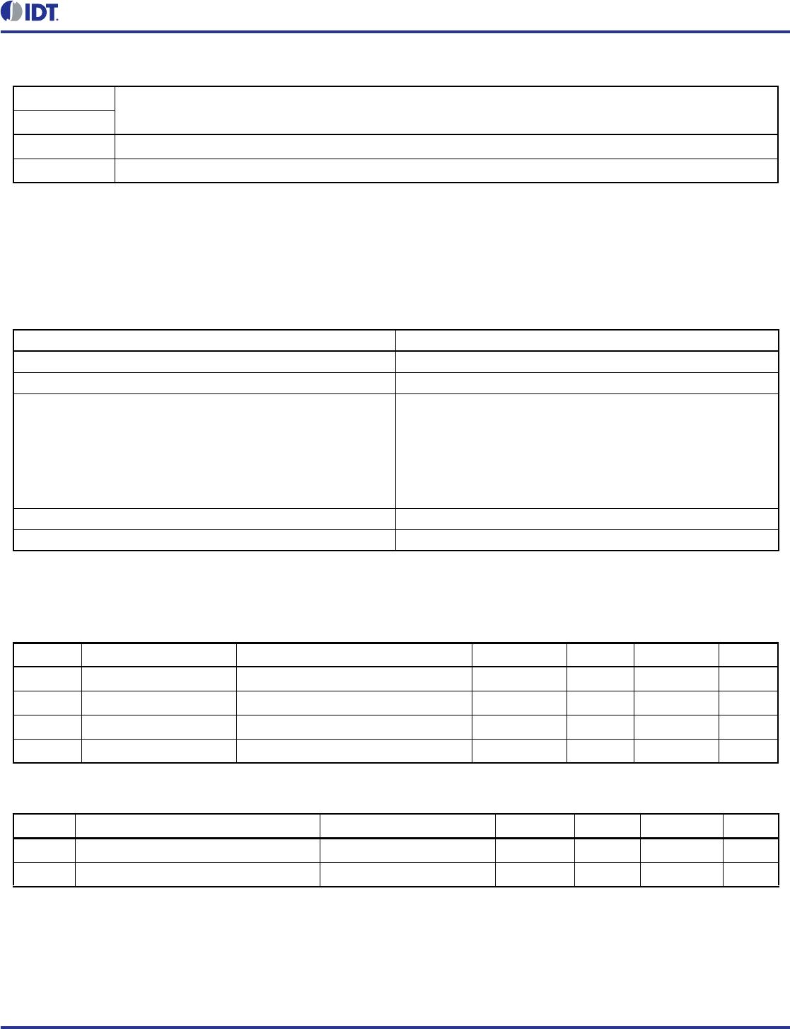
Table 3. Pin Characteristics
Function Tables
Table 4A. LOCK_DET Operation Table
Table 4B. STS12 Mode Configuration Table
Table 4C. LOCK_REFN Mode Configuration Table
Table 4D. SD Mode Configuration Table
Symbol Parameter Test Conditions Minimum Typical Maximum Units
C
IN
Input Capacitance 4 pF
R
PULLUP
Input Pullup Resistor 51 k
R
PULLDOWN
Input Pulldown Resistor 51 k
Operation
Output
LOCK_DET
The PLL is not locked to the serial input data stream if any of these three conditions occur:
A. Internal oscillator and REF_CLK input frequency are not within 500ppm of each other.
B. SD input is at logic LOW state.
C. LOCK_REFN is at logic LOW state.
LOW
When the PLL is locked to the serial input data stream, the CLK_OUT and DATA_OUT signals are valid. HIGH
Input
OperationSTS12
0
STM-1 (OC-3, STS-3) operation. The clock/data recovery circuit attempts to recover the clock from a 155.52 Mbit/s
input data stream. The output clock frequency is 155.52MHz.
1
STM-4 (OC-12, STS-12) operation. The clock/data recovery circuit attempts to recover the clock from a 622.08 Mbit/s
input data stream. The output clock frequency is 622.08MHz.
Input
OperationLOCK_REFN
0
Lock to reference clock. CLK_OUT/nCLK_OUT output frequency is within ±500ppm of the reference clock
(REF_CLK). DATA_OUT is set to logic LOW state and nDATA_OUT is set to logic HIGH state. (DATA_OUT = L,
nDATA_OUT = H).
1 Normal operation.
Input
OperationSD
0
Indicates a loss-of-signal (LOS) condition to the device. CLK_OUT/nCLK_OUT output frequency is within ±500ppm
of the reference clock (REF_CLK). DATA_OUT is set to logic LOW state and nDATA_OUT is set to logic HIGH state.
(DATA_OUT = L, nDATA_OUT = H).
1 Normal operation.
5©2016 Integrated Device Technology, Inc Revision C January 27, 2016
894D115I-04 Data Sheet
Table 4E. BYPASS Mode Configuration Table
Absolute Maximum Ratings
NOTE: Stresses beyond those listed under Absolute Maximum Ratings may cause permanent damage to the device.
These ratings are stress specifications only. Functional operation of product at these conditions or any conditions beyond
those listed in the DC Characteristics or AC Characteristics is not implied. Exposure to absolute maximum rating conditions for
extended periods may affect product reliability.
DC Electrical Characteristics
Table 5A. Power Supply DC Characteristics, V
DD
= 3.3V ± 5%, T = -40°C to 85°C
Table 5B. LVCMOS/LVTTL DC Characteristics, V
DD
= 3.3V ± 5%, T = -40°C to 85°C
Input
OperationBYPASS
0 Normal operation.
1 PLL bypassed (for factory test). The inverted REF_CLK input signal is output at CLK_OUT/nCLK_OUT.
Item Rating
Supply Voltage, V
DD
4.6V
Inputs, V
I
-0.5V to V
DD
+ 0.5V
Outputs, I
O
(LVDS)
Continuos Current
Surge Current
Outputs, I
O
(LVPECL)
Continuous Current
Surge Current
10mA
15mA
50mA
100mA
Package Thermal Impedance,
JA
81.3C/W (0 mps)
Storage Temperature, T
STG
-65C to 150C
Symbol Parameter Test Conditions Minimum Typical Maximum Units
V
DD
Core Supply Voltage 3.135 3.3 3.465 V
V
DDA
Analog Supply Voltage V
DD
– 0.10 3.3 V
DD
V
I
DD
Power Supply Current 112 mA
I
DDA
Analog Supply Current 10 mA
Symbol Parameter Test Conditions Minimum Typical Maximum Units
V
IH
Input High Voltage 2 V
DD
+ 0.3 V
V
IL
Input Low Voltage -0.3 0.8 V
6©2016 Integrated Device Technology, Inc Revision C January 27, 2016
894D115I-04 Data Sheet
Table 5C. Differential DC Characteristics, V
DD
= 3.3V ± 5%, T = -40°C to 85°C
Table 5D. LVPECL DC Characteristics, V
DD
= 3.3V ± 5%, T = -40°C to 85°C
NOTE 1: Outputs terminated with 50 to V
DD
– 2V.
Table 5E. LVDS DC Characteristics, V
DD
= 3.3V ± 5%, T = -40°C to 85°C
I
IH
Input High Current
REF_CLK,
STS12, BYPASS
V
DD
= V
IN
= 3.465V 150 µA
LOCK_REFN V
DD
= V
IN
= 3.465V 10 µA
I
IL
Input Low Current
REF_CLK,
STS12, BYPASS
V
DD
= 3.465V, V
IN
= 0V -10 µA
LOCK_REFN V
DD
= 3.465V, V
IN
= 0V -150 µA
Symbol Parameter Test Conditions Minimum Typical Maximum Units
I
IH
Input High Current DATA_IN/nDATA_IN V
DD
= V
IN
= 3.465V 150 µA
I
IL
Input Low Current
DATA_IN V
DD
= 3.465V, V
IN
= 0V -10 µA
nDATA_IN V
DD
= 3.465V, V
IN
= 0V -150 µA
V
IH
Input High Voltage V
DD
– 1.75 V
DD
– 0.4 V
V
IL
Input Low Voltage V
DD
– 2.0 V
DD
– 0.7 V
V
IN
Differential Input Voltage 250 mV
Symbol Parameter Test Conditions Minimum Typical Maximum Units
V
IH
Input High Voltage SD V
DD
– 1.125 V
V
IL
Input Low Voltage SD V
DD
– 1.5 V
I
IH
Input High Current SD V
DD
= V
IN
= 3.465V 150 µA
I
IL
Input Low Current SD V
DD
= 3.465V, V
IN
= 0V -10 µA
V
OH
Output High Voltage;
NOTE 1
LOCK_DT V
DD
– 1.4 V
DD
– 0.9 V
V
OL
Output Low Voltage
NOTE 1
LOCK_DT V
DD
– 2.0 V
DD
– 1.7 V
Symbol Parameter Test Conditions Minimum Typical Maximum Units
V
OD
Differential Output Voltage 247 380 454 mV
V
OD
V
OD
Magnitude Change 5 50 mV
V
OS
Offset Voltage 1.125 1.25 1.375 V
V
OS
V
OS
Magnitude Change 5 50 mV
Symbol Parameter Test Conditions Minimum Typical Maximum Units

894D115AGI-04LF

Mfr. #:
Manufacturer:
IDT
Description:
Clock Generators & Support Products STM-1/-4 OC-3/-12 CLK/DATA RECOVERY
Lifecycle:
New from this manufacturer.
Delivery:
DHL FedEx Ups TNT EMS
Payment:
T/T Paypal Visa MoneyGram Western Union

Products related to this Datasheet