Data Sheet ADG1406/ADG1407
Rev. C | Page 17 of 20
TERMINOLOGY
R
ON
Ohmic resistance between the D and S terminals.
ΔR
ON
Difference between the R
ON
of any two channels.
R
FLAT(ON)
Flatness is defined as the difference between the maximum
and minimum value of on resistance as measured.
I
S
(Off)
Source leakage current when the switch is off.
I
D
(Off)
Drain leakage current when the switch is off.
I
D
, I
S
(On)
Channel leakage current when the switch is on.
V
D
, V
S
Analog voltage on Terminal D and Terminal S.
C
S
(Off)
Channel input capacitance for the off condition.
C
D
(Off)
Channel output capacitance for the off condition.
C
D
, C
S
(On)
On switch capacitance.
C
IN
Digital input capacitance.
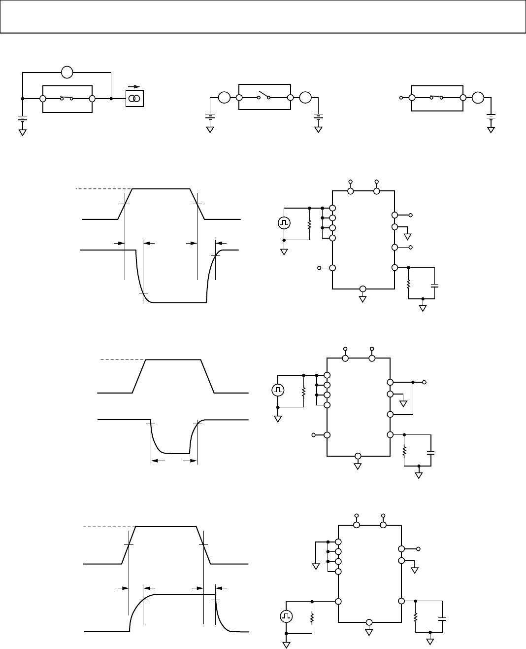
t
ON
(EN)
Delay time between the 50% and 90% points of the digital input
and the switch on condition.
t
OFF
(EN)
Delay time between the 50% and 90% points of the digital input
and the switch off condition.
t
TRANSITION
Delay time between the 50% and 90% points of the digital
inputs and the switch on condition when switching from one
address state to another.
t
BBM
Off time measured between the 80% points of the switches
when switching from one address state to another.
V
INL
Maximum input voltage for Logic 0.
V
INH
Minimum input voltage for Logic 1.
I
INL
, I
INH
Input current of the digital input.
I
DD
Positive supply current.
I
SS
Negative supply current.
Off Isolation
A measure of unwanted signal coupling through an off channel.
Charge Injection
A measure of the glitch impulse transferred from the digital
input to the analog output during switching.
Bandwidth
The frequency at which the output is attenuated by 3 dB.
On Response
The frequency response of the on switch.
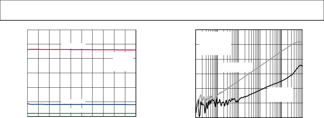
Total Harmonic Distortion Plus Noise (THD + N)
The ratio of the harmonic amplitude plus noise of the signal to
the fundamental.
AC Power Supply Rejection Ratio (ACPSRR)
Measures the ability of a device to avoid coupling noise and
spurious signals that appear on the supply voltage pin to the
output of the switch. The dc voltage on the device is modu-
lated by a sine wave of 0.62 V p-p. The ratio of the amplitude
of signal on the output to the amplitude of the modulation is
the ACPSRR.