Data Sheet ADG1406/ADG1407
Rev. C | Page 7 of 20
Parameter +25°C
−40°C to
+85°C
−40°C to
+125°C
1
Unit Test Conditions/Comments
POWER REQUIREMENTS V
DD
= +5.5 V, V
SS
= −5.5 V
I
DD
0.002 μA typ Digital inputs = 0 V or V
DD
1 μA max
I
SS
0.002 μA typ Digital inputs = 0 V, 5 V, or V
DD
1 μA max
V
DD
/V
SS
±4.5/±16.5 V min/max
1
Temperature range for B version: −40°C to +125°C.
2
Guaranteed by design, not subject to production test.
CONTINUOUS CURRENT PER CHANNEL
Table 5. Continuous Current per Channel (ADG1406)
Parameter 25°C 85°C 125°C Unit Test Conditions/Comments
CONTINUOUS CURRENT PER CHANNEL
1
15 V Dual Supply V
DD
= +13.5 V, V
SS
= −13.5 V
28-Lead TSSOP 180 100 50 mA max
32-Lead LFCSP 300 150 60 mA max
12 V Single Supply V
DD
= 10.8 V, V
SS
= 0 V
28-Lead TSSOP 150 90 50 mA max
32-Lead LFCSP 260 130 55 mA max
5 V Dual Supply V
DD
= +4.5 V, V
SS
= −4.5 V
28-Lead TSSOP 140 85 45 mA max
32-Lead LFCSP 245 130 55 mA max
1
Guaranteed by design, not subject to production test.
Table 6. Continuous Current per Channel (ADG1407)
Parameter 25°C 85°C 125°C Unit Test Conditions/Comments
CONTINUOUS CURRENT PER CHANNEL
1
15 V Dual Supply V
DD
= +13.5 V, V
SS
= −13.5 V
28-Lead TSSOP 135 85 45 mA max
32-Lead LFCSP 235 125 55 mA max
12 V Single Supply V
DD
= 10.8 V, V
SS
= 0 V
28-Lead TSSOP 110 70 40 mA max
32-Lead LFCSP 190 110 50 mA max
5 V Dual Supply V
DD
= +4.5 V, V
SS
= −4.5 V
28-Lead TSSOP 105 65 40 mA max
32-Lead LFCSP 180 100 50 mA max
1
Guaranteed by design, not subject to production test.
ADG1406/ADG1407 Data Sheet
Rev. C | Page 8 of 20
ABSOLUTE MAXIMUM RATINGS
T
A
= 25°C, unless otherwise noted.
Table 7.
Parameter Rating
V
DD
to V
SS
35 V
V
DD
to GND −0.3 V to +25 V
V
SS
to GND +0.3 V to −25 V
Analog Inputs
1
V
SS
− 0.3 V to V
DD
+ 0.3 V or
30 mA, whichever occurs first
Digital Inputs
1
GND − 0.3 V to V
DD
+ 0.3 V or
30 mA, whichever occurs first
Continuous Current, Sx or Dx Pins
Table 5 and Table 6
specifications + 15%
Peak Current, Sx or Dx Pins
(Pulsed at 1 ms, 10% Duty
Cycle Maximum)
28-Lead TSSOP 300 mA
32-Lead LFCSP 550 mA
Operating Temperature Range
Industrial (B Version) −40°C to +125°C
Storage Temperature Range −65°C to +150°C
Junction Temperature 150°C
Reflow Soldering, Pb-Free
Peak Temperature 260 (+0/−5)°C
Time at Peak Temperature 10 sec to 40 sec
1
Overvoltages at the Ax, EN, Sx, or Dx pins are clamped by internal diodes.
Limit current to the maximum ratings given.
Stresses at or above those listed under Absolute Maximum
Ratings may cause permanent damage to the product. This is a
stress rating only; functional operation of the product at these
or any other conditions above those indicated in the operational
section of this specification is not implied. Operation beyond
the maximum operating conditions for extended periods may
affect product reliability.
Only one absolute maximum rating may be applied at any
one time.
THERMAL RESISTANCE
θ
JA
is specified for the worst-case conditions, that is, a device
soldered in a circuit board for surface-mount packages.
Table 8. Thermal Resistance
Package Type θ
JA
θ
JC
Unit
28-Lead TSSOP 97.9 14 °C/W
32-Lead LFCSP 27.27 °C/W
ESD CAUTION
Data Sheet ADG1406/ADG1407
Rev. C | Page 9 of 20
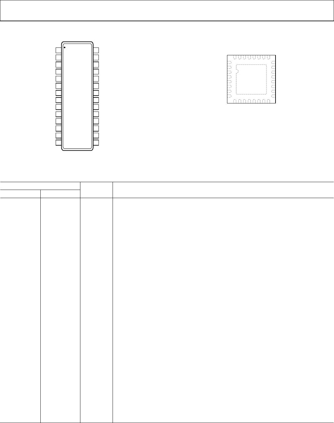
PIN CONFIGURATIONS AND FUNCTION DESCRIPTIONS
1
V
DD
28
D
2
NC
27
V
SS
3
NC
26
S8
4
S16
25
S7
5
S15
24
S6
6
S14
23
S5
7
S13
22
S4
8
S12
21
S3
9
S11
20
S2
10
S10
19
S1
11
S9
18
EN
12
G
ND
17
A0
13
NC
16
A1
14
A3
15
A2
ADG1406
TOP VIEW
(Not to Scale)
NC = NO CONNECT
07419-003
Figure 3. ADG1406 TSSOP Pin Configuration
07419-004
S16
S15
S14
S13
S12
S11
S10
S9
S8
S7
S6
S5
S4
S3
S2
S1
G
ND
A3
A2
NC
NC
A1
A0
EN
NC
V
DD
NC
D
NC
NC
NC
V
SS
1. NC = NO CONNECT. DO NOT CONNECT
TO THIS PIN.
2. THE EXPOSED PAD MUST BE TIED TO
THE SUBSTRATE, V
SS
.
24
23
22
21
20
19
18
17
1
2
3
4
5
6
7
8
9
10
11
12
13
14
15
16
32
31
30
29
28
27
26
25
ADG1406
TOP VIEW
(Not to Scale)
Figure 4. ADG1406 LFCSP Pin Configuration
Table 9. ADG1406 Pin Function Descriptions
Pin No.
TSSOP LFCSP Mnemonic Description
1 31 V
DD
Most Positive Power Supply Potential.
2, 3, 13
12, 13, 26, 27,
28, 30, 32
NC No Connect.
4 1 S16 Source Terminal 16. This pin can be an input or an output.
5 2 S15 Source Terminal 15. This pin can be an input or an output.
6 3 S14 Source Terminal 14. This pin can be an input or an output.
7 4 S13 Source Terminal 13. This pin can be an input or an output.
8 5 S12 Source Terminal 12. This pin can be an input or an output.
9 6 S11 Source Terminal 11. This pin can be an input or an output.
10 7 S10 Source Terminal 10. This pin can be an input or an output.
11 8 S9 Source Terminal 9. This pin can be an input or an output.
12 9 GND Ground (0 V) Reference.
14 10 A3 Logic Control Input.
15 11 A2 Logic Control Input.
16 14 A1 Logic Control Input.
17 15 A0 Logic Control Input.
18 16 EN
Active High Digital Input. When this pin is low, the device is disabled and all switches are
turned off. When this pin is high, the Ax logic inputs determine which switch is turned on.
19 17 S1 Source Terminal 1. This pin can be an input or an output.
20 18 S2 Source Terminal 2. This pin can be an input or an output.
21 19 S3 Source Terminal 3. This pin can be an input or an output.
22 20 S4 Source Terminal 4. This pin can be an input or an output.
23 21 S5 Source Terminal 5. This pin can be an input or an output.
24 22 S6 Source Terminal 6. This pin can be an input or an output.
25 23 S7 Source Terminal 7. This pin can be an input or an output.
26 24 S8 Source Terminal 8. This pin can be an input or an output.
27 25 V
SS
Most Negative Power Supply Potential. In single-supply applications, this pin can be
connected to ground.
28 29 D Drain Terminal. This pin can be an input or an output.
Not applicable 0 EPAD Exposed Pad. The exposed pad must be tied to the substrate, V
SS
.

ADG1407BRUZ

Mfr. #:
Manufacturer:
Analog Devices Inc.
Description:
Multiplexer Switch ICs 8:1 110MHz 9.5 Ohm iCMOS
Lifecycle:
New from this manufacturer.
Delivery:
DHL FedEx Ups TNT EMS
Payment:
T/T Paypal Visa MoneyGram Western Union