10
Electrical Specifications
0°C T
A
70°C, 4.5 V V
CC
20 V, 1.6 mA I
F(ON)
5 mA, 0 V V
F(OFF)
0.8 V, unless otherwise
specified. All Typicals at T
A
= 25°C. See note 8.
Device
Parameter Symbol HCPL- Min. Typ.* Max. Units Test Conditions Fig. Note
Current CTR 800 3500 25k % I
F
= 40 µA, V
O
= 0.4 V 4, 5 2
Transfer V
CC
= 4.5 V
600 3000 8k I
F
= 0.5 mA,
V
CC
= 4.5 V
700 3200 25k I
F
= 40 µA
500 2700 8k I
F
= 0.5 mA
Logic Low V
OL
0.06 0.4 V I
F
= 40 µA, I
O
= 280 µA 2, 3
0.04 0.4 I
F
= 0.5 mA, I
O
= 2.5 mA
Logic High I
OH
0.01 5 µAV
O
= V
CC
= 3 to 7 V,
Output Current I
F
= 0 mA
0.02 80 V
O
= V
CC
= 18 V,
I
F
= 0 mA
Logic Low I
CCL
4701/070A 0.02 0.2 mA I
F
= 40 µAV
O
= Open
0.1 1 I
F
= 0.5 mA
4731/073A 0.04 0.4 I
F
= 40 µA
0.2 2.0 I
F
= 0.5 mA
Logic High I
CCH
4701/070A <0.01 10 µAI
F
= 0 mA V
O
= Open
4731/073A <0.01 20
Input Forward V
F
1.1 1.25 1.4 V I
F
= 40 to 500 µA, 6
Voltage T
A
= 25°C
0.95 1.5 I
F
= 40 to 500 µA
Input Reverse BV
R
3.0 5.0 V I
R
= 100 µA, T
A
= 25°C
2.5 I
R
= 100 µA
Temperature V
F
/T
A
-2.0 mV/°CI
F
= 40 µA
-1.6 I
F
= 0.5 mA
Input Capacitance C
IN
18 pF f = 1 MHz, V
F
= 0 V
*All typical values at T
A
= 25°C and V
CC
= 5 V, unless otherwise noted.
Ratio
Supply Current
Supply Current
Output Voltage
Coefficient of
Forward Voltage
Breakdown
Voltage
11
Package Characteristics
Device
Parameter Symbol HCPL- Min. Typ.* Max. Units Test Conditions Fig. Note
Input-Output Momentary V
ISO
3750 V rms RH 50%, 3, 4
Withstand Voltage** t = 1 min.,
Option 020 4701 5000 3, 4a
4731
Resistance R
I-O
10
12
V
I-O
= 500 VDC 3
(Input-Output) RH 45%
Capacitance C
I-O
0.6 pF f = 1 MHz 3
(Input-Output)
Insulation Leakage I
I-I
4731 0.005 µARH 45%, t = 5 s, 5
Current (Input-Input) 073A V
I-I
= 500 VDC
Resistance (Input-Input) R
I-I
10
11
Capacitance C
I-I
4731 0.03 pF f = 1 MHz 5
(Input-Input) 073A 0.25
*All typical values at T
A
= 25°C and V
CC
= 5 V.
**The Input-Output Momentary Withstand Voltage is a dielectric voltage rating that should not be interpreted as an input-output
continuous voltage rating. For the continuous voltage rating refer to the IEC/EN/DIN EN 60747-5-2 Insulation Characteristics
Table (if applicable), your equipment level safety specification or Avago Application Note 1074 entitled “Optocoupler Input-Output
Endurance Voltage.”
Switching Specifications (AC)
Over Recommended Operating Conditions T
A
= 0°C to 70°C, V
CC
= 3 V to 18 V, unless otherwise specified.
Device
Parameter Symbol HCPL- Min. Typ.* Max. Units Test Conditions Fig. Note
Propagation t
PHL
65 500 µsI
F
= 40 µA, R
L
= 11 to 16 k,7, 99, 10
Delay Time V
CC
= 3.3 to 5 V
325 T
A
= 25°C I
F
= 0.5 mA,
30
Propagation t
PLH
70 500 µsI
F
= 40 µA, R
L
= 11 to 16 k,7, 99, 10
Delay Time V
CC
= 3.3 to 5 V
34 60 T
A
= 25°C I
F
= 0.5 mA,
4701/4731 90
070A/073A 130
Common Mode |CM
H
|1,000 10,000 V/µsI
F
= 0 mA, R
L
= 4.7 to 11 k,86, 7
Transient V
CM
= 10 V
p-p
,
Immunity at T
A
= 25°C,
Logic High
Output
Common Mode |CM
L
|1,000 10,000 V/µsI
F
= 0.5 mA, R
L
= 4.7 to 11 k,86, 7
Transient |V
CM
| = 10 V
p-p
,
Immunity at T
A
= 25°C
2,000 I
F
= 40 µA, R
L
= 11 to 16 k,
|V
CM
| = 10 V
p-p
V
CC
= 3.3 to 5 V, T
A
= 25°C
*All typical values at T
A
= 25°C and V
CC
= 5 V, unless otherwise noted.
to Logic Low
at Output
R
L
= 4.7 k
to Logic High
Output
R
L
= 4.7 k
Logic Low
Output
T
A
= 25°C
12
Notes:
1. Specification information is available
form the factory for 1.6 V operation.
Call your local field sales office for
further information.
2. DC CURRENT TRANSFER RATIO is
defined as the ratio of output
collector current, I
O
, to the forward
LED input current, I
F
, times 100%.
3. Device considered a two terminal
device: pins 1, 2, 3, and 4 shorted
together, and pins 5, 6, 7, and 8
shorted together.
4. In accordance with UL 1577, each
optocoupler is proof tested by
applying an insulation test voltage
4500 V
RMS
for 1 second (leakage
detection current limit, I
I-O
5 µA.
4a. In accordance with UL 1577, each
optocoupler is proof tested by
applying an insulation test voltage
6000 V
RMS
for 1 second (leakage
detection current limit, I
I-O
5 µA.
This test is performed before the
100% production test for partial
discharge (Method b) shown in the
IEC/EN/DIN EN 60747-5-2 Insulation
Characteristics Table.
5. Measured between pins 1 and 2
shorted together, and pins 3 and 4
shorted together.
6. Common transient immunity in a
Logic High level is the maximum
tolerable (positive) dV
CM
/dt on the
leading edge of the common mode
pulse, V
CM
, to assure that the output
will remain in a Logic High state (i.e.,
V
O
> 2.0 V). Common transient
immunity in a Logic Low level is he
maximum tolerable (negative)
dV
CM
/dt on the trailing edge of the
common mode pulse, V
CM
, to assure
that the output will remain in a Logic
Low state (i.e., V
O
< 0.8 V).
7. In applications where dV/dt may
exceed 50,000 V/µs (such as static
discharge) a series resistor, R
CC
,
should be included to protect the
detector IC form destructively high
surge currents. The recommended
value is R
CC
= 220 .
8. Use of a 0.1 µF bypass capacitor con-
nected between pins 8 and 5 adjacent
to the device is recommended.
9. Pin 7 open for single channel product.
10. Use of resistor between pins 5 and 7
will decrease gain and delay time.
Significant reduction in overall gain
can occur when using resistor values
below 47 k for single channel
product.
11. The Applications Information section
of this data sheet references the
HCPL-47XX part family, but applies
equally to the HCPL-070A and HCPL-
073A parts.
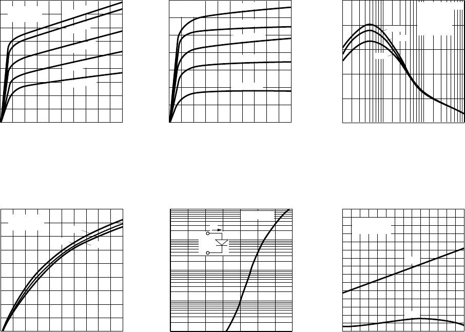
Figure 2. DC Transfer Characteristics
(I
F
= 0.5 mA to 2.5 mA).
Figure 3. DC Transfer Characteristics
(I
F
= 50 µA to 250 µA).
Figure 4. Current Transfer Ratio vs.
Forward Current.
Figure 5. Output Current vs. Input
Diode Forward Current.
Figure 6. Input Diode Forward
Current vs. Forward Voltage.
Figure 7. Propagation Delay vs.
Temperature.
I
O
– OUTPUT CURRENT – mA
0
7
0
V
O
– OUTPUT VOLTAGE – V
2.0
6
5
4
3
2
1
1.0
T
A
= 25°C
V
CC
= 5 V
I
F
= 250
µA
I
F
= 200
µA
I
F
= 150
µA
I
F
= 100
µA
I
F
= 50 µA
I
F
– FORWARD CURRENT – mA
0.8
0.01
V
F
– FORWARD VOLTAGE
1.5
10
1.0
0.1
0.9 1.3
100
1.0 1.1 1.2 1.4
T
A
= 25°C
I
F
V
F
+
I
O
– OUTPUT CURRENT – mA
0
27
0
V
O
– OUTPUT VOLTAGE – V
2.0
24
21
18
15
12
9
6
3
1.0
T
A
= 25°C
V
CC
= 5 V
I
F
= 2.5 m
A
I
F
= 2.0 mA
I
F
= 1.5 mA
I
F
= 1.0 mA
I
F
= 0.5 m
A
NORMALIZED CURRENT TRANSFER RATIO
0.01
1.25
0
I
F
– FORWARD CURRENT – mA
10
0.75
0.5
0.25
0.1 1.0
1.0
25°C
70°C
0°C
NORMALIZED
I
F
= 40 µA
V
O
= 0.4 V
V
CC
= 5 V
I
O
– OUTPUT CURRENT – mA
0
9
0
I
F
– INPUT DIODE FORWARD CURRENT – mA
0.5
8
7
6
5
4
3
2
1
0.1
V
O
= 0.4 V
V
CC
= 5 V
0.2 0.3 0.4
25°C
0°C
70°C
I
P
– PROPAGATION DELAY – µs
0
0
T
A
– TEMPERATURE – °C
70
70
60
50
40
30
20
10
50
I
F
= 0.5 mA
R
L
= 4.7 k
10 20 30 40 60
t
PLH
t
PHL

HCPL-4731#300

Mfr. #:
Manufacturer:
Broadcom / Avago
Description:
High Speed Optocouplers 2Ch 10mA 600mW
Lifecycle:
New from this manufacturer.
Delivery:
DHL FedEx Ups TNT EMS
Payment:
T/T Paypal Visa MoneyGram Western Union