7
Regulatory Information
The HCPL-4701/4731 and HCPL-
070A/073A have been approved
by the following organizations:
UL
Recognized under UL 1577,
Component Recognition
Program, File E55361.
CSA
Approved under CSA Component
Acceptance Notice #5, File CA
88324.
IEC/EN/DIN EN 60747-5-2
Approved under:
IEC 60747-5-2:1997 + A1:2002
EN 60747-5-2:2001 + A1:2002
DIN EN 60747-5-2 (VDE 0884
Teil 2):2003-01.
(Option 060 only)
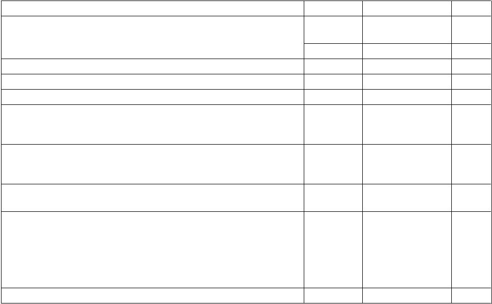
Insulation Related Specifications
8-Pin DIP
(300 Mil) SO-8
Parameter Symbol Value Value Units Conditions
Minimum External Air L(101) 7.1 4.9 mm Measured from input terminals to
Gap (External output terminals, shortest distance
Clearance) through air.
Minimum External L(102) 7.4 4.8 mm Measured from input terminals to
Tracking (External output terminals, shortest distance
Creepage) path along body.
Minimum Internal Plastic 0.08 0.08 mm Through insulation distance, conductor
Gap (Internal Clearance) to conductor, usually the direct
distance between the photoemitter and
photodetector inside the optocoupler
cavity.
Tracking Resistance CTI 200 200 Volts DIN IEC 112/ VDE 0303 Part 1
(Comparative Tracking
Index)
Isolation Group IIIa IIIa Material Group DIN VDE 0110,
1/89, Table 1)
Option 300 – surface mount classification is Class A in accordance with CECC 00802.
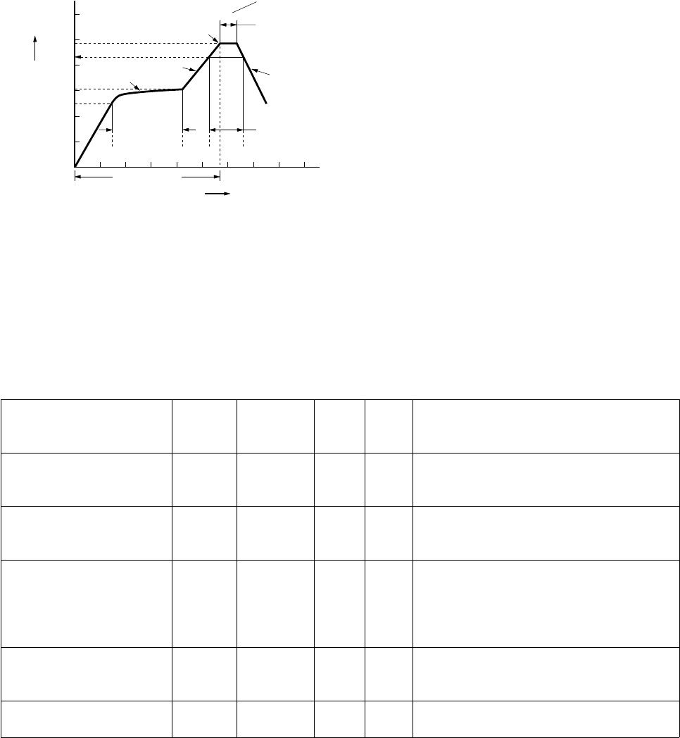
Figure 1b. Pb-Free IR Profile.
Recommended Pb-Free IR Profile
217 °C
RAMP-DOWN
6 °C/SEC. MAX.
RAMP-UP
3 °C/SEC. MAX.
150 - 200 °C
260 +0/-5 °C
t 25 °C to PEAK
60 to 150 SEC.
20-40 SEC.
TIME WITHIN 5 °C of ACTUAL
PEAK TEMPERATURE
t
p
t
s
PREHEAT
60 to 180 SEC.
t
L
T
L
T
smax
T
smin
25
T
p
TIME
TEMPERATURE
NOTES:
THE TIME FROM 25 °C to PEAK TEMPERATURE = 8 MINUTES MAX.
T
smax
= 200 °C, T
smin
= 150 °C
Note: Non-halide flux should be used.
8
IEC/EN/DIN EN 60747-5-2 Insulation Related Characteristics (HCPL-4701 OPTION 060 ONLY)
Description Symbol Characteristic Units
Installation classification per DIN VDE 0110/1.89, Table 1
for rated mains voltage 300 V rms I-IV
for rated mains voltage 450 V rms I-III
Climatic Classification 55/85/21
Pollution Degree (DIN VDE 0110/1.89) 2
Maximum Working Insulation Voltage V
IORM
630 V peak
Input to Output Test Voltage, Method b*
V
IORM
x 1.87 = V
PR
, 100% Production Test with t
m
= 1 sec, V
PR
1181 V peak
Partial Discharge < 5 pC
Input to Output Test Voltage, Method a*
V
IORM
x 1.5 = V
PR
, Type and sample test, V
PR
945 V peak
t
m
= 60 sec, Partial Discharge < 5 pC
Highest Allowable Overvoltage*
(Transient Overvoltage, t
ini
= 10 sec) V
IOTM
6000 V peak
Safety Limiting Values
(Maximum values allowed in the event of a failure,
also see Figure 16, Thermal Derating curve.)
Case Temperature T
S
175 °C
Input Current I
S,INPUT
230 mA
Output Power P
S,OUTPUT
600 mW
Insulation Resistance at T
S
, V
IO
= 500 V R
S
>10
9
*Refer to the front of the optocoupler section of the current catalog, under Product Safety Regulations section, IEC/EN/DIN EN
60747-5-2, for a detailed description.
Note: Isolation characteristics are guaranteed only within the safety maximum ratings which must be ensured by protective circuits in
application.
9
Absolute Maximum Ratings
(No Derating Required up to 70°C)
Parameter Symbol Minimum Maximum Units
Storage Temperature T
S
-55 125 °C
Operating Temperature T
A
-40 85 °C
Average Forward Input Current (HCPL-4701/4731) I
F(AVG)
10 mA
Average Forward Input Current (HCPL-070A/073A) I
F(AVG)
5mA
Peak Transient Input Current (HCPL-4701/4731) I
FPK
20 mA
(50% Duty Cycle, 1 ms Pulse Width)
Peak Transient Input Current (HCPL-070A/073A) I
FPK
10 mA
(50% Duty Cycle, 1 ms Pulse Width)
Reverse Input Voltage V
R
2.5 V
Input Power Dissipation (Each Channel) P
I
15 mW
Output Current (Each Channel) I
O
60 mA
Emitter Base Reverse Voltage (HCPL-4701/070A) V
EB
0.5 V
Output Transistor Base Current (HCPL-4701/070A) I
B
5mA
Supply Voltage V
CC
-0.5 18 V
Output Voltage V
O
-0.5 18 V
Output Power Dissipation (Each Channel) P
O
100 mW
Total Power Dissipation (Each Channel) P
T
115 mW
Lead Solder Temperature (for Through Hole Devices) 260°C for 10 sec., 1.6 mm below seating plane
Reflow Temperature Profile See Package Outline Drawings section
(for SOIC-8 and Option #300)
Recommended Operating Conditions
Parameter Symbol Min. Max. Units
Power Supply Voltage V
CC
* 1.6 18 V
Forward Input Current (ON) I
F(ON)
40 5000 µA
Forward Input Voltage (OFF) V
F(OFF)
0 0.8 V
Operating Temperature T
A
070 °C
*See Note 1.

HCPL-4731#300

Mfr. #:
Manufacturer:
Broadcom / Avago
Description:
High Speed Optocouplers 2Ch 10mA 600mW
Lifecycle:
New from this manufacturer.
Delivery:
DHL FedEx Ups TNT EMS
Payment:
T/T Paypal Visa MoneyGram Western Union