2008-2016 Microchip Technology Inc. DS20002122D-page 1
11AA02E48/11AA02E64
Device Selection Table
Features
Pre-Programmed Globally Unique, 48-Bit or
64-Bit Node Address
Compatible with EUI-48
and EUI-64
Single I/O, UNI/O
®
Serial Interface Bus
Low-Power CMOS Technology:
- 1 mA active current, typical
- 1 µA standby current, maximum
256 x 8-Bit Organization
Schmitt Trigger Inputs for Noise Suppression
Output Slope Control to Eliminate Ground Bounce
100 kbps Maximum Bit Rate – Equivalent to
100 kHz Clock Frequency
Self-Timed Write Cycle (including Auto-Erase)
Page-Write Buffer for up to 16 Bytes
STATUS Register for Added Control:
- Write Enable Latch bit
- Write-In-Progress bit
Block Write Protection:
- Protect none, 1/4, 1/2 or all of array
Built-in Write Protection:
- Power-on/off data protection circuitry
- Write enable latch
High Reliability:
- Endurance: 1,000,000 erase/write cycles
- Data retention: >200 years
- ESD protection: >4,000V
3-Lead SOT-23 and 8-Lead SOIC Packages
Pb-Free and RoHS Compliant
Available Temperature Ranges:
Description
The Microchip Technology Inc.
11AA02E48/11AA02E64 (11AA02EXX
(1)
) device is a
2 Kbit Serial Electrically Erasable PROM. The device is
organized in blocks of x8-bit memory and support the
patented
(2)
single I/O UNI/O
®
serial bus. By using
Manchester encoding techniques, the clock and data
are combined into a single, serial bit stream (SCIO),
where the clock signal is extracted by the receiver to
correctly decode the timing and value of each bit.
Low-voltage design permits operation down to 1.8V,
with standby and active currents of only 1 µA and
1 mA, respectively.
The 11AA02EXX is available in standard 8-lead
SOIC and 3-lead SOT-23 packages.
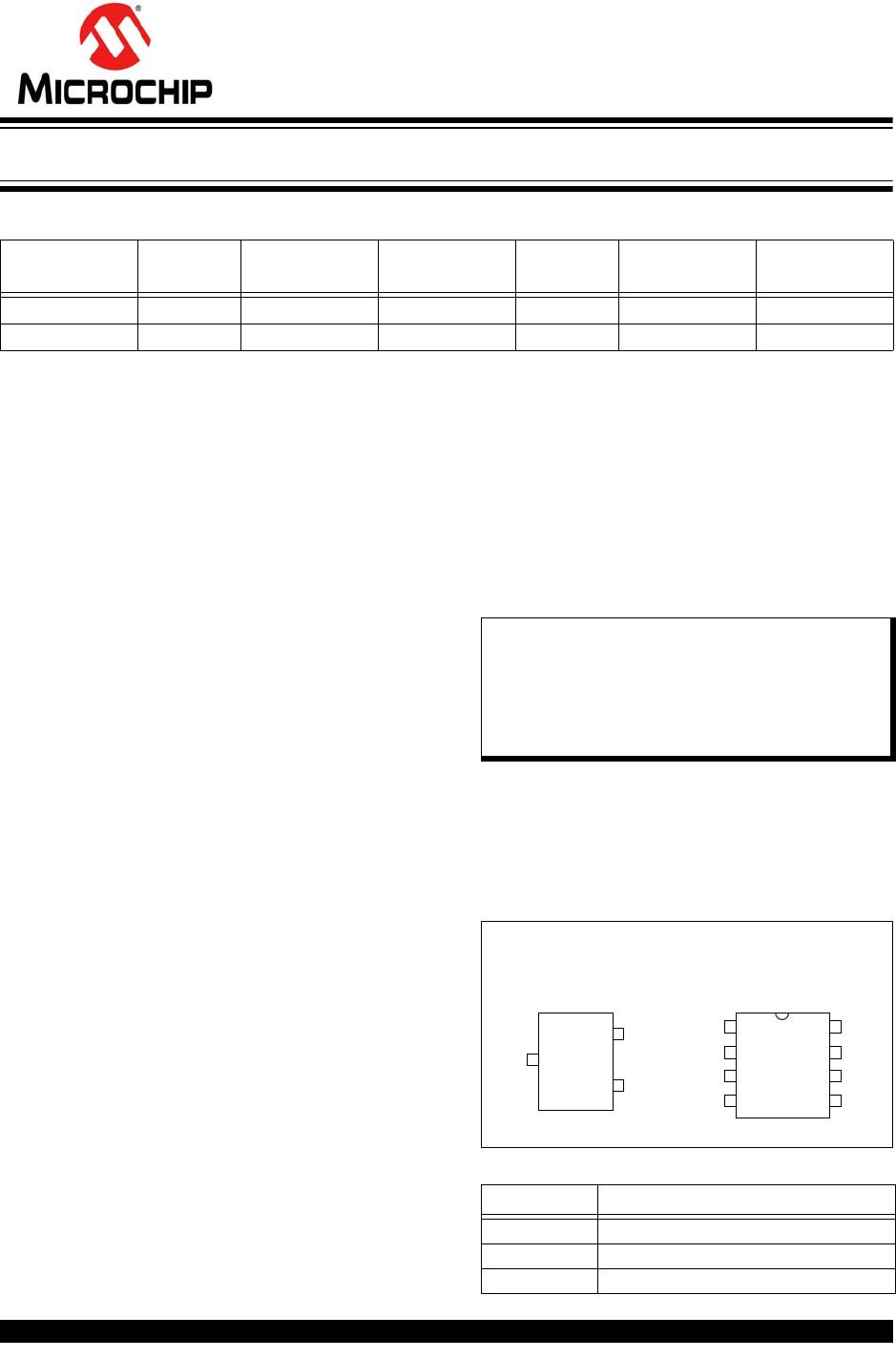
Package Types (not to scale)
Pin Function Table
Part Number
Density
(bits)
VCC Range
Page Size
(Bytes)
Temp.
Ranges
Packages Node Address
11AA02E48 2K 1.8V-5.5V 16 I SN, TT EUI-48
11AA02E64 2K 1.8V-5.5V 16 I SN, TT EUI-64
- Industrial (I): -40°C to +85°C
Note 1: 11AA02EXX is used in this document as
a generic part number for the 11AA02E48
and 11AA02E64 devices.
2: Microchip’s UNI/O
®
Bus products are
covered by the following patents issued
in the U.S.A.: 7,376,020 and 7,788,430.
Name Function
SCIO
Serial Clock, Data Input/Output
V
SS Ground
V
CC Supply Voltage
VCC
SCIO
V
SS
3-Lead SOT-23
(TT)
NC
NC
NC
V
SS
V
CC
NC
NC
SCIO
1
2
3
4
8
7
6
5
SOIC
(SN)
3
2
1
2K UNI/O
®
Serial EEPROMs with EUI-48
or EUI-64
Node Identity
11AA02E48/11AA02E64
DS20002122D-page 2 2008-2016 Microchip Technology Inc.
1.0 ELECTRICAL CHARACTERISTICS
Absolute Maximum Ratings
(†)
VCC.............................................................................................................................................................................6.5V
SCIO w.r.t. V
SS.................................................................................................................................... -0.6V to VCC+1.0V
Storage temperature .................................................................................................................................-65°C to 150°C
Ambient temperature under bias.................................................................................................................-40°C to 85°C
ESD protection on all pins..........................................................................................................................................4 kV
TABLE 1-1: DC CHARACTERISTICS
† NOTICE: Stresses above those listed under ‘Absolute Maximum Ratings’ may cause permanent damage to the
device. This is a stress rating only and functional operation of the device at those or any other conditions above those
indicated in the operational listings of this specification is not implied. Exposure to maximum rating conditions for an
extended period of time may affect device reliability.
DC CHARACTERISTICS
Electrical Characteristics:
Industrial (I): VCC = 2.5V to 5.5V TA = -40°C to +85°C
V
CC = 1.8V to 2.5V TA = -20°C to +85°C
Param.
No.
Symbol Characteristic Min. Max. Units Test Conditions
D1 V
IH High-Level Input
Voltage
0.7 VCC VCC+1 V
D2 V
IL Low-Level Input
Voltage
-0.3 0.3 VCC VVCC 2.5V
-0.3 0.2 V
CC VVCC <2.5V
D3 VHYS Hysteresis of Schmitt
Trigger Inputs
(SCIO)
0.05 Vcc V VCC 2.5V (Note 1)
D4 VOH High-Level Output
Voltage
VCC -0.5 V IOH =-300µA, VCC =5.5V
VCC -0.5 V IOH = -200 µA, Vcc = 2.5V
D5 V
OL Low-Level Output
Voltage
—0.4VIOI=300µA, VCC =5.5V
—0.4VIOI = 200 µA, Vcc = 2.5V
D6 IO Output Current Limit
(Note 2)
—±4mAVCC = 5.5V (Note 1)
—±3mAVcc = 2.5V (Note 1)
D7 I
LI Input Leakage
Current (SCIO)
—±1µAVIN = VSS or VCC
D8 CINT Internal Capacitance
(all inputs and
outputs)
—7pFT
A = 25°C, FCLK = 1 MHz,
V
CC = 5.0V (Note 1)
D9 I
CCREAD Read Operating
Current
—3mAVCC = 5.5V, FBUS =100kHz,
C
B = 100 pF
—1mAV
CC = 2.5V, FBUS =100kHz,
C
B = 100 pF
D10 ICCWRITE Write Operating
Current
—5mAVCC =5.5V
—3mAV
CC =2.5V
D11 Iccs Standby Current 1 µA V
CC =5.5V, TA =85°C
D12 I
CCI Idle Mode Current 50 µA VCC =5.5V
Note 1: This parameter is periodically sampled and not 100% tested.
2: The SCIO output driver impedance will vary to ensure IO is not exceeded.
2008-2016 Microchip Technology Inc. DS20002122D-page 3
11AA02E48/11AA02E64
TABLE 1-3: AC TEST CONDITIONS
TABLE 1-2: AC CHARACTERISTICS
AC CHARACTERISTICS
Electrical Characteristics:
Industrial (I): VCC = 2.5V to 5.5V TA = -40°C to +85°C
V
CC = 1.8V to 2.5V TA = -20°C to +85°C
Param.
No.
Symbol Characteristic Min. Max. Units Test Conditions
1F
BUS Serial Bus
Frequency
10 100 kHz
2T
E Bit Period 10 100 µs
3TIJIT Input Edge Jitter
To l er an c e
±0.06 UI Note 2
4F
DRIFT Serial Bus
Frequency Drift Rate
To l er an c e
±0.50 % per byte
5F
DEV Serial Bus
Frequency Drift Limit
±5 % per command
6T
OJIT Output Edge Jitter ±0.25 UI Note 2
7T
R SCIO Input Rise
Time (Note 1)
100 ns
8T
F SCIO Input Fall Time
(Note 1)
100 ns
9T
STBY Standby Pulse Time 600 µs
10 TSS Start Header Setup
Time
10 µs
11 T
HDR Start Header Low
Pulse Time
5— µs
12 T
SP Input Filter Spike
Suppression (SCIO)
—50 ns Note 1
13 T
WC Write Cycle Time
(byte or page)
5 ms Write, WRSR commands
10 ms ERAL, SETAL commands
14 Endurance (per
page)
1M cycles 25°C, V
CC =5.5V (Note 3)
Note 1: This parameter is periodically sampled and not 100% tested.
2: A Unit Interval (UI) is equal to 1-bit period (T
E) at the current bus frequency.
3: This parameter is not tested but ensured by characterization. For endurance estimates in a specific
application, please consult the Total Endurance
Model which can be obtained on Microchip’s website:
www.microchip.com.
AC Waveform
VLO = 0.2V
V
HI = VCC - 0.2V
C
L = 100 pF
Timing Measurement Reference Level
Input 0.5 V
CC
Output 0.5 VCC

11AA02E48-I/SN

Mfr. #:
Manufacturer:
Microchip Technology
Description:
EEPROM 2K, 256x8, 1.8V MAC Addressable
Lifecycle:
New from this manufacturer.
Delivery:
DHL FedEx Ups TNT EMS
Payment:
T/T Paypal Visa MoneyGram Western Union