2008-2016 Microchip Technology Inc. DS20002122D-page 13
11AA02E48/11AA02E64
4.5 Read Status Register (RDSR)
Instruction
The RDSR instruction provides access to the STATUS
register. The STATUS register may be read at any time,
even during a write cycle. The STATUS register is
formatted as follows:
The Write-In-Process (WIP) bit indicates whether the
11AA02EXX is busy with a write operation. When set to
a ‘1’, a write is in progress, when set to a ‘0’, no write is
in progress. This bit is read-only.
The Write Enable Latch (WEL) bit indicates the status
of the write enable latch. When set to a ‘1’, the latch
allows writes to the array, when set to a ‘0’, the latch
prohibits writes to the array. This bit is set and cleared
using the WREN and WRDI instructions, respectively.
This bit is read-only for any other instruction.
The Block Protection (BP0 and BP1) bits indicate
which blocks are currently write-protected. These bits
are set by the user through the WRSR instruction. These
bits are nonvolatile.
The WIP and WEL bits will update dynamically
(asynchronous to issuing the RDSR instruction).
Furthermore, after the STATUS register data is
received, the master can provide a MAK during the
Acknowledge sequence to request that the data be
transmitted again. This allows the master to
continuously monitor the WIP and WEL bits without the
need to issue another full command.
Once the master is finished, it provides a NoMAK to
end the operation.
FIGURE 4-6: READ STATUS REGISTER COMMAND SEQUENCE
7654 3 2 1 0
XXXX BP1 BP0 WEL WIP
Note: Bits 4-7 are don’t cares, and will read as0’.
Note: If Read Status Register command is
initiated while the 11AA02EXX is currently
executing an internal write cycle on the
STATUS register, the new Block
Protection bit values will be read during
the entire command.
Note: The current drawn for a Read Status
Register command during a write cycle is
a combination of the I
CC Read and ICC
Write operating currents.
11010100
Start Header
SCIO
Device Address
MAK
00001010
MAK
Command
11000000
MAK
NoSAK
SAK
Standby Pulse
SCIO
SAK
STATUS Register Data
3210
NoMAK
SAK
The STATUS register data can continuously be read or polled by transmitting a MAK in place of the NoMAK.Note:
0000
11AA02E48/11AA02E64
DS20002122D-page 14 2008-2016 Microchip Technology Inc.
4.6 Write Status Register (WRSR)
Instruction
The WRSR instruction allows the user to select one of
four levels of protection for the array by writing to the
appropriate bits in the STATUS register. The array is
divided up into four segments. The user has the ability
to write-protect none, one, two, or all four of the
segments of the array. The partitioning is controlled as
illustrated in Table 4- 3.
After transmitting the STATUS register data, the master
must transmit a NoMAK during the Acknowledge
sequence in order to initiate the internal write cycle.
TABLE 4-3: ARRAY PROTECTION
FIGURE 4-7: WRITE STATUS REGISTER COMMAND SEQUENCE
Note: The WRSR instruction must be terminated
with a NoMAK following the data byte. If a
NoMAK is not received at this point, the
command will be considered invalid, and
the device will go into Idle mode without
responding with a SAK or executing the
command.
BP1 BP0
Array Addresses
Write-Protected
00 none
01 upper 1/4
(C0h-FFh)
10 upper 1/2
(80h-FFh)
11 all
(00h-FFh)
11010100
Start Header
SCIO
Device Address
MAK
00001010
MAK
Command
10101101
MAK
NoSAK
SAK
Standby Pulse
SCIO
SAK
7654
Status Register Data
3210
NoMAK
SAK
Twc
2008-2016 Microchip Technology Inc. DS20002122D-page 15
11AA02E48/11AA02E64
4.7 Erase All (ERAL) Instruction
The ERAL instruction allows the user to write ‘0x00’ to
the entire memory array with one command. Note that
the write enable latch (WEL) must first be set by issuing
the WREN instruction.
Once the write enable latch is set, the user may
proceed with issuing a ERAL instruction (including the
header and device address bytes). Immediately after
the NoMAK bit has been transmitted by the master, the
internal write cycle is initiated, during which time all
words of the memory array are written to ‘0x00’.
The ERAL instruction is ignored if either of the Block
Protect bits (BP0, BP1) are not 0, meaning 1/4, 1/2 or
all of the array is protected.
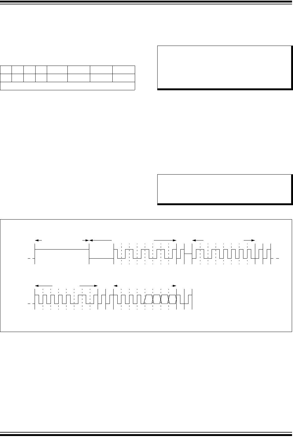
FIGURE 4-8: ERASE ALL COMMAND SEQUENCE
4.8 Set All (SETAL) Instruction
The SETAL instruction allows the user to write ‘0xFF’ to
the entire memory array with one command. Note that
the write enable latch (WEL) must first be set by issuing
the WREN instruction.
Once the write enable latch is set, the user may
proceed with issuing a SETAL instruction (including the
header and device address bytes). Immediately after
the NoMAK bit has been transmitted by the master, the
internal write cycle is initiated, during which time all
words of the memory array are written to ‘0xFF.
The SETAL instruction is ignored if either of the Block
Protect bits (BP0, BP1) is not0’, meaning 1/4, 1/2 or
all of the array is protected.
FIGURE 4-9: SET ALL COMMAND SEQUENCE
Note: The ERAL instruction must be terminated
with a NoMAK following the command
byte. If a NoMAK is not received at this
point, the command will be considered
invalid, and the device will go into Idle
mode without responding with a SAK or
executing the command.
11010100
Start Header
SCIO
Device Address
MAK
00001010
MAK
Command
11101100
NoMAK
NoSAK
SAK
Standby Pulse
SCIO
SAK
Twc
Note: The SETAL instruction must be terminated
with a NoMAK following the command
byte. If a NoMAK is not received at this
point, the command will be considered
invalid, and the device will go into Idle
mode without responding with a SAK or
executing the command.
11010100
Start Header
SCIO
Device Address
MAK
00001010
MAK
Command
11001101
NoMAK
NoSAK
SAK
Standby Pulse
SCIO
SAK
Twc

11AA02E48-I/SN

Mfr. #:
Manufacturer:
Microchip Technology
Description:
EEPROM 2K, 256x8, 1.8V MAC Addressable
Lifecycle:
New from this manufacturer.
Delivery:
DHL FedEx Ups TNT EMS
Payment:
T/T Paypal Visa MoneyGram Western Union