11AA02E48/11AA02E64
DS20002122D-page 10 2008-2016 Microchip Technology Inc.
4.2 Current Address Read (CRRD)
Instruction
The internal address counter featured on the
11AA02EXX maintains the address of the last memory
array location accessed. The CRRD instruction allows
the master to read data back beginning from this
current location. Consequently, no word address is
provided upon issuing this command.
Note that, except for the initial word address, the READ
and CRRD instructions are identical, including the
ability to continue requesting data through the use of
MAKs in order to sequentially read from the array.
As with the READ instruction, the CRRD instruction is
terminated by transmitting a NoMAK.
Table 4-2 lists the events upon which the internal
address counter is modified.
TABLE 4-2: INTERNAL ADDRESS
COUNTER
FIGURE 4-2: CRRD COMMAND SEQUENCE
Command Event Action
Power-on Reset Counter is undefined
READ or
WRITE
MAK edge
following each
Address byte
Counter is updated
with newly received
value
READ,
WRITE, or
CRRD
MAK/NoMAK
edge following
each data byte
Counter is
incremented by 1
Note: If, following each data byte in a READ,
WRITE, or CRRD instruction, neither a
MAK nor a NoMAK edge is received
(i.e., if a standby pulse occurs instead),
the internal address counter will not be
incremented.
Note: During a Write command, once the last
data byte for a page has been loaded, the
internal Address Pointer will rollover to the
beginning of the selected page.
7654
Data Byte 1
3210 7654
Data Byte 2
3210
7654
Data Byte n
3210
SCIO
MAK
MAK
NoMAK
11010100
Start Header
SCIO
Device Address
MAK
00001010
MAK
Command
10000001
MAK
NoSAK
SAK
Standby Pulse
SCIO
SAK
SAK
SAK
SAK
2008-2016 Microchip Technology Inc. DS20002122D-page 11
11AA02E48/11AA02E64
4.3 Write Instruction
Prior to any attempt to write data to the 11AA02EXX,
the write enable latch must be set by issuing the WREN
instruction (see Section 4.4 “Write Enable (WREN)
and Write Disable (WRDI) Instructions”).
Once the write enable latch is set, the user may
proceed with issuing a WRITE instruction (including the
header and device address bytes) followed by the MSB
and LSB of the Word Address. Once the last
Acknowledge sequence has been performed, the
master transmits the data byte to be written.
The 11AA02EXX features a 16-byte page buffer,
meaning that up to 16 bytes can be written at one time.
To utilize this feature, the master can transmit up to
16 data bytes to the 11AA02EXX, which are
temporarily stored in the page buffer. After each data
byte, the master sends a MAK, indicating whether or
not another data byte is to follow. A NoMAK indicates
that no more data is to follow, and as such will initiate
the internal write cycle.
Upon receipt of each word, the four lower-order
Address Pointer bits are internally incremented by one.
The higher-order bits of the word address remain
constant. If the master should transmit data past the
end of the page, the address counter will roll over to the
beginning of the page, where further received data will
be written.
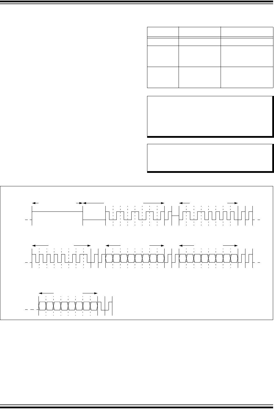
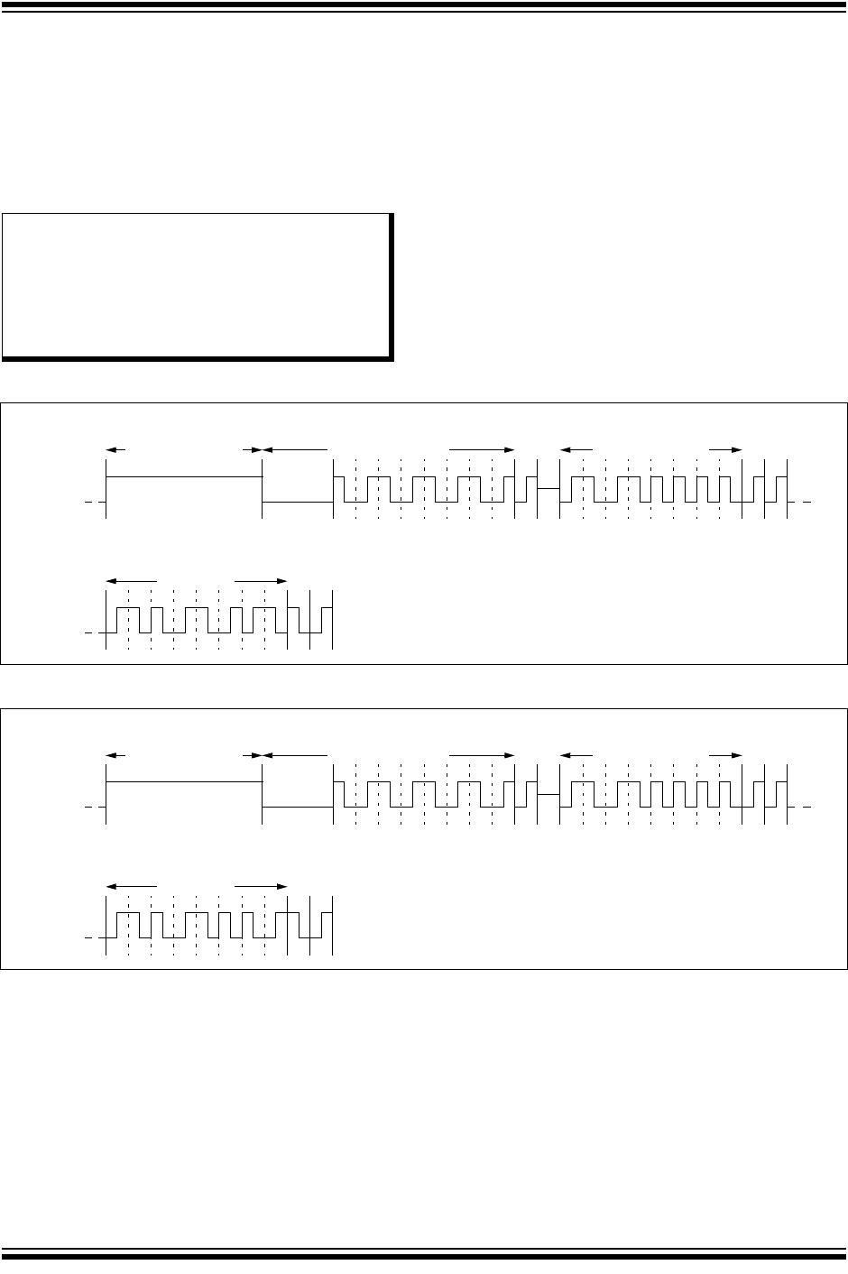
FIGURE 4-3: WRITE COMMAND SEQUENCE
Note: If a NoMAK is generated before any data
has been provided, or if a standby pulse
occurs before the NoMAK is generated,
the 11AA02EXX will be reset, and the
write cycle will not be initiated.
Note: Page write operations are limited to
writing bytes within a single physical page,
regardless of the number of bytes
actually being written. Physical page
boundaries start at addresses that are
integer multiples of the page size
(16 bytes) and end at addresses that are
integer multiples of the page size minus 1.
As an example, the page that begins at
address 0x30 ends at address 0x3F. If a
page Write command attempts to write
across a physical page boundary, the
result is that the data wraps around to the
beginning of the current page (overwriting
data previously stored there), instead of
being written to the next page as might be
expected. It is therefore necessary for the
application software to prevent page write
operations that would attempt to cross a
page boundary.
7654
Data Byte 1
3210
7654
Data Byte 2
3210
7654
Data Byte n
3210
SCIO
MAK
MAK
No MAK
11010100
Start Header
SCIO
Device Address
MAK
00001010
MAK
Command
10101100
MAK
NoSAK
SAK
Standby Pulse
SCIO
SAK
15 14 13 12
Word Address MSB
11 10 9 8
MAK
SAK
7654
Word Address LSB
3210
MAK
SAK
SAK
SAK
SAK
Twc
11AA02E48/11AA02E64
DS20002122D-page 12 2008-2016 Microchip Technology Inc.
4.4 Write Enable (WREN) and Write
Disable (WRDI) Instructions
The 11AA02EXX contains a write enable latch. See
Table 6-1 for the Write-Protect Functionality Matrix.
This latch must be set before any write operation will be
completed internally. The WREN instruction will set the
latch, and the WRDI instruction will reset the latch.
The following is a list of conditions under which the
write enable latch will be reset:
Power-up
WRDI instruction successfully executed
WRSR instruction successfully executed
WRITE instruction successfully executed
ERAL instruction successfully executed
SETAL instruction successfully executed
FIGURE 4-4: WRITE ENABLE COMMAND SEQUENCE
FIGURE 4-5: WRITE DISABLE COMMAND SEQUENCE
Note: The WREN and WRDI instructions must be
terminated with a NoMAK following the
command byte. If a NoMAK is not
received at this point, the command will be
considered invalid, and the device will go
into Idle mode without responding with a
SAK or executing the command.
11010100
Start Header
SCIO
Device Address
MAK
00001010
MAK
Command
10010011
NoMAK
NoSAK
SAK
Standby Pulse
SCIO
SAK
11010100
Start Header
SCIO
Device Address
MAK
00001010
MAK
Command
01010010
NoMAK
NoSAK
SAK
Standby Pulse
SCIO
SAK

11AA02E48-I/SN

Mfr. #:
Manufacturer:
Microchip Technology
Description:
EEPROM 2K, 256x8, 1.8V MAC Addressable
Lifecycle:
New from this manufacturer.
Delivery:
DHL FedEx Ups TNT EMS
Payment:
T/T Paypal Visa MoneyGram Western Union