11AA02E48/11AA02E64
DS20002122D-page 6 2008-2016 Microchip Technology Inc.
3.0 BUS CHARACTERISTICS
3.1 Standby Pulse
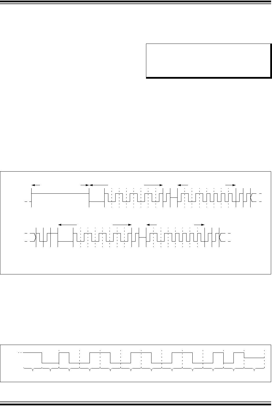
When the master has control of SCIO, a standby pulse
can be generated by holding SCIO high for T
STBY. At
this time, the 11AA02EXX will reset and return to
Standby mode. Subsequently, a high-to-low transition
on SCIO (the first low pulse of the header) will return
the device to the active state.
Once a command is terminated satisfactorily (i.e., via
a NoMAK/SAK combination during the Acknowledge
sequence), performing a standby pulse is not required
to begin a new command as long as the device to be
selected is the same device selected during the
previous command. However, a period of T
SS must be
observed after the end of the command and before the
beginning of the start header. After TSS, the start
header (including T
HDR low pulse) can be transmitted
in order to begin the new command.
If a command is terminated in any manner other than a
NoMAK/SAK combination, then the master must
perform a standby pulse before beginning a new
command, regardless of which device is to be selected
.
An example of two consecutive commands is shown in
Figure 3-1. Note that the device address is the same
for both commands, indicating that the same device is
being selected both times.
A standby pulse cannot be generated while the slave
has control of SCIO. In this situation, the master must
wait for the slave to finish transmitting and to release
SCIO before the pulse can be generated.
If, at any point during a command, an error is detected
by the master, a standby pulse should be generated
and the command should be performed again.
FIGURE 3-1: CONSECUTIVE COMMANDS EXAMPLE
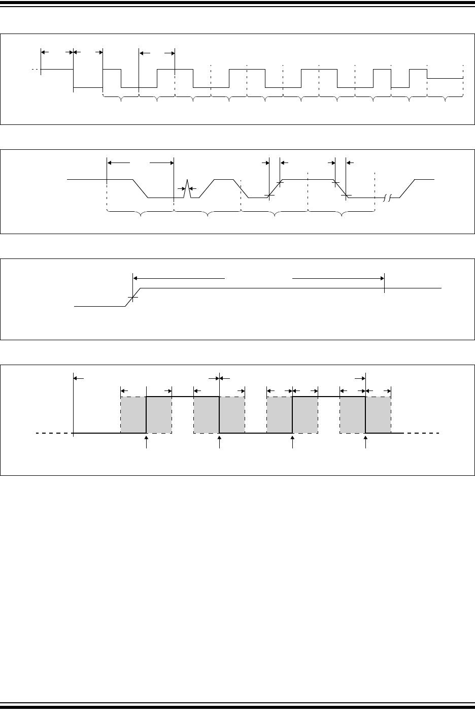
3.2 Start Data Transfer
All operations must be preceded by a start header. The
start header consists of holding SCIO low for a period
of THDR, followed by transmitting an 8-bit ‘01010101’
code. This code is used to synchronize the slave’s
internal clock period with the master’s clock period, so
accurate timing is very important.
When a standby pulse is not required (i.e., between
successive commands to the same device), a period of
T
SS must be observed after the end of the command
and before the beginning of the start header.
Figure 3-2 shows the waveform for the start header,
including the required Acknowledge sequence at the
end of the byte.
FIGURE 3-2: START HEADER
Note: After a POR/BOR event occurs, a
low-to-high transition on SCIO must be
generated before proceeding with
communication, including a standby
pulse.
11010100
Start Header
SCIO
Device Address
MAK
00001010
MAK
NoSAK
SAK
Standby Pulse
(1)
11010100
Start Header
SCIO
Device Address
MAK
00001010
MAK
NoSAK
SAK
NoMAK
SAK
TSS
Note 1: After a POR/BOR event, a low-to-high transition on SCIO is required to occur before the first
standby pulse.
SCIO
Data ‘0’ Data ‘1’ Data ‘0’ Data ‘1’ Data ‘0’ Data ‘1’ Data ‘0’ Data ‘1’ MAK NoSAKTSS THDR