10
425112fd
LTC4251/LTC4251-1/
LTC4251-2
For more information www.linear.com/4251
Two modes of operation are possible during the time the
MOSFET is first turning on, depending on the values of
external components, MOSFET characteristics and nomi-
nal design current. One possibility is that the MOSFET
will turn on gradually so that the inrush into the load
capacitance remains a low value. The output will simply
ramp to –48V and the MOSFET will be fully enhanced.
A second possibility is that the load current exceeds the
current limit threshold of 100mV/R
S
. In this case, the
LTC4251/LTC4251-1/LTC4251-2 will ramp the output by
sourcing 100mV/R
S
current into the load capacitance.
It is important to set the timer delay so that, regardless
of which start-up mode is used, the start-up time is less
than the TIMER delay time. If this condition is not met,
the LTC4251/LTC4251-1/LTC4251-2 may shutdown after
one TIMER delay.
Board Removal
If the board is withdrawn from the card cage, the UV/OV
divider is the first to lose connection. This shuts off the
MOSFET and commutates the flow of current in the con-
nector. When the power pins subsequently separate, there
is no arcing.
Current Control
Three levels of protection handle short-circuit and over-
load conditions. Load current is monitored by SENSE and
resistor R
S
. There are three distinct thresholds at SENSE:
50mV for a timed circuit breaker function; 100mV for an
analog current limit loop; and 200mV for a fast, feedfor-
ward comparator which limits peak current in the event
of a catastrophic short-circuit.
If, owing to an output overload, the voltage drop across R
S
exceeds 50mV, TIMER sources 230µA into C
T
. C
T
eventually
charges to a 4V threshold and the LTC4251/LTC4251-1/
LTC4251-2 latchoff. If the overload goes away and SENSE
measures less than 50mV, C
T
slowly discharges (5.8µA).
OPERATION
In this way the circuit breaker function will also respond
to low duty cycle overloads, and accounts for fast heating
and slow cooling characteristic of the MOSFET.
Higher overloads are handled by an analog current limit
loop. If the drop across R
S
reaches 100mV, the current
limiting loop servos the MOSFET gate and maintains a
constant output current of 100mV/R
S
. Note that because
SENSE > 50mV, TIMER charges C
T
during this time and the
LTC4251/LTC4251-1/LTC4251-2 will eventually shut down.
Low impedance failures on the load side of the LTC4251/
LTC4251-1/LTC4251-2 coupled with 48V or more driving
potential can produce current slew rates well in excess of
50A/µs. Under these conditions, overshoot is inevitable. A
fast SENSE comparator with a threshold of 200mV detects
overshoot and pulls GATE low much harder and hence
much faster than can the weaker current limit loop. The
100mV/R
S
current limit loop then takes over, and servos
the current as previously described. As before, TIMER
runs and latches the LTC4251/LTC4251-1/LTC4251-2 off
when C
T
reaches 4V.
The LTC4251/LTC4251-1/LTC4251-2 circuit breaker latch
is reset by either pulling UV/OV momentarily low, or
dropping the input voltage V
IN
below the internal UVLO
threshold of 8.2V.
Although short-circuits are the most obvious fault type,
several operating conditions may invoke overcurrent
protection. Noise spikes from the backplane or load, input
steps caused by the connection of a second, higher voltage
supply, transient currents caused by faults on adjacent
circuit boards sharing the same power bus, or the insertion
of non-hot swappable products could cause higher than
anticipated input current and temporary detection of an
overcurrent condition. The action of TIMER and C
T
rejects
these events allowing the LTC4251/LTC4251-1/LTC4251-2
to “ride out” temporary overloads and disturbances that
would trip a simple current comparator and in some cases,
blow a fuse.
11
425112fd
LTC4251/LTC4251-1/
LTC4251-2
For more information www.linear.com/4251
SHUNT REGULATOR
A fast responding shunt regulator clamps the V
IN
pin to
13V (V
Z
). Power is derived from –48RTN by an external
current limiting resistor, R
IN
. A 1µF decoupling capacitor,
C
IN
filters supply transients and contributes a short delay
at start-up.
To meet creepage requirements R
IN
may be split into two
or more series connected units, such as two 5.1k or three
3.3k resistors. This introduces a wider total spacing than is
possible with a single component while at the same time
ballasting the potential across the gap under each resistor.
The LTC4251 is fundamentally a low voltage device that
operates with –48V as its reference ground. To further
protect against arc discharge into its pins, the area in and
around the LTC4251 and all associated components should
be free of any other planes such as chassis ground, return,
or secondary-side power and ground planes.
V
IN
is rated handle 30mA within the thermal limits of the
package, and is tested to survive a 100µs, 100mA pulse. To
protect V
IN
against damage from higher amplitude spikes,
clamp V
IN
to V
EE
with a 13V Zener diode. Star connect
V
EE
and all V
EE
referred components to the sense resistor
Kelvin terminal as illustrated in Figure 2, keeping trace
lengths between V
IN
, C
IN
, D
IN
and V
EE
as short as possible.
INTERNAL UNDERVOLTAGE LOCKOUT (UVLO)
Internal circuitry monitors V
IN
for undervoltage. The exact
thresholds are defined by V
LKO
and its hysteresis, V
LKH
.
When V
IN
rises above 9.2V (V
LKO
) the chip is enabled;
below 8.2V (V
LKO
-V
LKH
) it is disabled and GATE is pulled
low. The UVLO function at V
IN
should not be confused with
the UV/OV pin. These are completely separate functions.
UV/OV COMPARATORS
Two hysteretic comparators for detecting under- and
overvoltage conditions, with the following thresholds,
monitor the dual function UV/OV pin:
UV turning on at V
UVHI
UV turning off at V
UVLO
APPLICATIONS INFORMATION
OV turning off at V
OVHI
OV turning on at V
OVLO
The UV and OV trip point ratio for LTC4251 is designed to
match the standard telecom operating range of 43V to 75V.
The LTC4251-2 implements a UV threshold of 43V only.
A divider (R1, R2) is used to scale the supply voltage. Using
R1 = 402k and R2 = 32.4k gives a typical operating range
of 43.2V to 74.4V. The under- and overvoltage shutdown
thresholds are then 39.2V and 82.5V. 1% divider resis-
tors are recommended to preserve threshold accuracy.
The same resistor values can be used for the LTC4251-2.
The R1-R2 divider values shown in the Typical Application
set a standing current of slightly more than 100µA, and
define an impedance at UV/OV of 30k. In most applications,
30k impedance coupled with 300mV UV hysteresis makes
the LTC4251/LTC4251-1/LTC4251-2 insensitive to noise. If
more noise immunity is desired, add a 1nF to 10nF filter
capacitor from UV/OV to V
EE
.
The UV and OV trip point thresholds for the LTC4251-1 are
designed to encompass the standard telecom operating
range of –36V to –72V.
A divider (R1, R2) is used to scale the supply voltage.
Using R1 = 442k and R2 = 34.8k gives a typical operating
range of 33.2V to 81V. The typical under- and overvoltage
shutdown thresholds are then 29.6V and 84.5V. 1% divider
resistors are recommended to preserve threshold accuracy.
The R1-R2 divider values shown in the Typical Application
set a standing current of slightly more than 100µA, and
define an impedance at UV/OV of 32k. In most applica-
tions, 32k impedance coupled with 260mV UV hysteresis
makes the LTC4251-1 insensitive to noise. If more noise
immunity is desired, add a 1nF to 10nF filter capacitor
from UV/OV to V
EE
.
UV/OV OPERATION
A low input to the UV comparator will reset the chip and
pull the GATE and TIMER pins low. A low-to-high UV
transition will initiate an initial timing sequence if the three
remaining interlock conditions are met.
12
425112fd
LTC4251/LTC4251-1/
LTC4251-2
For more information www.linear.com/4251
Overvoltage conditions detected by the OV comparator
will also pull GATE low, thereby shutting down the load,
but it will not reset the circuit breaker latch. Returning the
supply voltage to an acceptable range restarts the GATE
pin provided all interlock conditions except TIMER are met.
TIMER
The operation of the TIMER pin is somewhat complex as
it handles several key functions. A capacitor, C
T
, is used
at TIMER to provide timing for the LTC4251/LTC4251-1/
LTC4251-2. Four different charging and discharging modes
are available at TIMER:
1. 5.8µA slow charge; initial timing delay
2. 230µA fast charge; circuit breaker delay
3. 5.8µA slow discharge; circuit breaker “cool-off”
4. Low impedance switch; resets capacitor after initial
timing delay, in undervoltage lockout, and in overvoltage
For initial startup, the 5.8µA pull-up is used. The low im-
pedance switch is turned off and the 5.8µA current source
is enabled when the four interlock conditions are met. C
T
charges to 4V in a time period given by:
t =
4V C
T
5.8µA
(1)
When C
T
reaches 4V (V
TMRH
), the low impedance switch
turns on and discharges C
T
. The GATE output is enabled
and the load turns on.
CIRCUIT BREAKER TIMER OPERATION
If the SENSE pin detects more than 50mV across R
S
,
the TIMER pin charges C
T
with 230µA. If C
T
charges to
4V, the GATE pin pulls low and the LTC4251/LTC4251-1/
LTC4251-2 latch off. The part remains latched off until
either the UV/OV pin is momentarily pulsed low, or V
IN
dips into UVLO and is then restored. The circuit breaker
timeout period is given by
t =
4V C
T
230µA
(2)
Intermittent overloads may exceed the 50mV threshold
at SENSE, but if their duration is sufficiently short TIMER
will not reach 4V and the LTC4251/LTC4251-1/LTC4251-2
will not latch off. To handle this situation, the TIMER
discharges C
T
slowly with a 5.8µA pull-down whenever
the SENSE voltage is less than 50mV. Therefore any in-
termittent overload with an aggregate duty cycle of 2.5%
or more will eventually trip the circuit breaker and latch
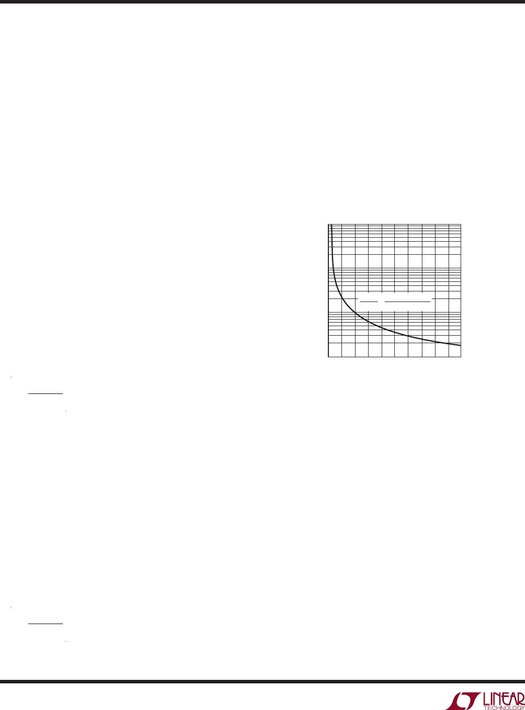
off the LTC4251/LTC4251-1/LTC4251-2. Figure 3 shows
the circuit breaker response time in seconds normalized
to 1µF. The asymmetric charging and discharging of C
T
is
a fair gauge of MOSFET heating.
APPLICATIONS INFORMATION
GATE
GATE is pulled low to V
EE
under any of the following
conditions: in UVLO, during the initial timing cycle, in an
overvoltage condition, or when the LTC4251/LTC4251-1/
LTC4251-2 are latched off after a short-circuit. When GATE
turns on, a 58µA current source charges the MOSFET gate
and any associated external capacitance. V
IN
limits gate
drive to no more than 14.5V.
Gate-drain capacitance (C
GD
) feed through at the first
abrupt application of power can cause a gate-source
voltage sufficient to turn on the MOSFET. A unique circuit
pulls GATE low with practically no usable voltage at V
IN
,
and eliminates current spikes at insertion. A large external
gate-source capacitor is thus unnecessary for the purpose
of compensating C
GD
. Instead, a smaller value (≥10nF)
capacitor C
C
is adequate. C
C
also provides compensation
for the analog current limit loop.
Figure 3. Circuit Breaker Response Time
FAULT DUTY CYCLE, D (%)
20 40 60 800
NORMALIZED RESPONSE TIME (s/µF)
10
1
0.1
0.01
100
425112 F03
t
C
T
(µF)
4
(235.8 • D) – 5.8
=

LTC4251-1IS6#TRPBF

Mfr. #:
Manufacturer:
Analog Devices Inc.
Description:
Hot Swap Voltage Controllers Neg V Hot Swap Cntrs in SOT-23
Lifecycle:
New from this manufacturer.
Delivery:
DHL FedEx Ups TNT EMS
Payment:
T/T Paypal Visa MoneyGram Western Union