13
425112fd
LTC4251/LTC4251-1/
LTC4251-2
For more information www.linear.com/4251
SENSE
The SENSE pin is monitored by the circuit breaker (CB)
comparator, the analog current limit (ACL) amplifier, and
the fast current limit (FCL) comparator. Each of these
three measures the potential of SENSE relative to V
EE
. If
SENSE exceeds 50mV, the CB comparator activates the
230µA TIMER pull-up. At 100mV, the ACL amplifier servos
the MOSFET current, and at 200mV the FCL compara-
tor abruptly pulls GATE low in an attempt to bring the
MOSFET current under control. If any of these conditions
persists long enough for TIMER to charge C
T
to 4V (see
Equation(2)), the LTC4251/LTC4251-1/LTC4251-2 latch
off and pull GATE low.
If the SENSE pin encounters a voltage greater than 100mV,
the ACL amplifier will servo GATE downwards in an attempt
to control the MOSFET current. Since GATE overdrives the
MOSFET in normal operation, the ACL amplifier needs time
to discharge GATE to the threshold of the MOSFET. For a
mild overload, the ACL amplifier can control the MOSFET
current, but in the event of a severe overload the current
may overshoot. At SENSE = 200mV, the FCL comparator
takes over, quickly discharging the GATE pin to near V
EE
potential. FCL then releases, and the ACL amplifier takes
over. All the while TIMER is running. The effect of FCL is
to add a nonlinear response to the control loop in favor
of reducing MOSFET current.
Owing to inductive effects in the system, FCL typically
overcorrects the current limit loop, and GATE undershoots.
A zero in the loop (resistor R
C
in series with the gate
capacitor) helps the ACL amplifier recover.
SHORT-CIRCUIT OPERATION
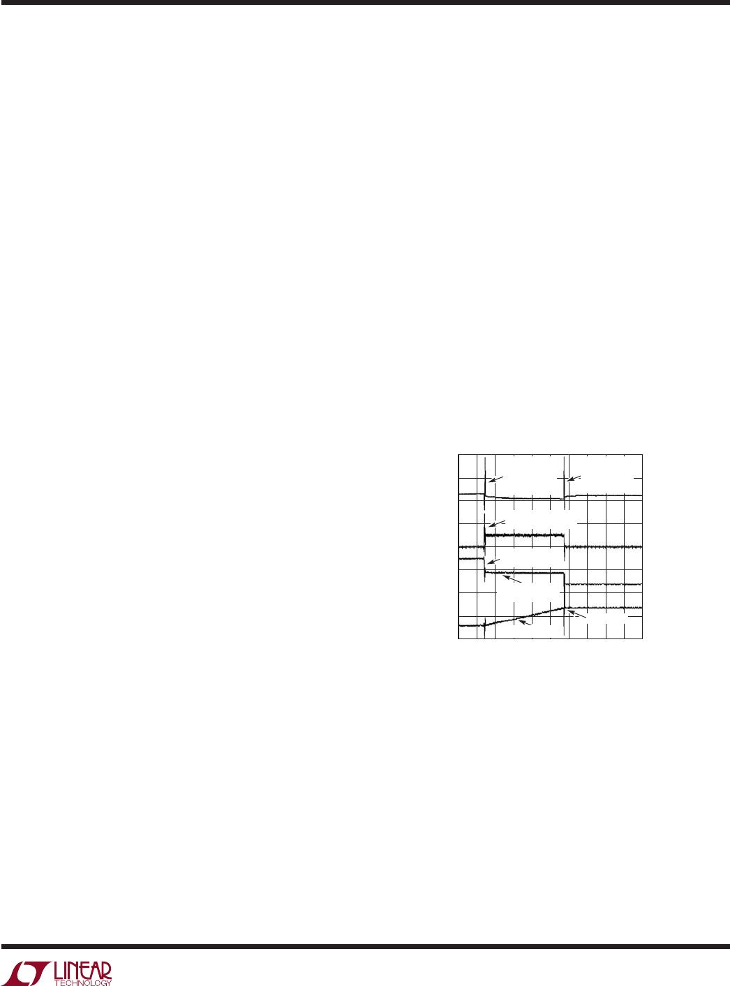
Circuit behavior arising from a load-side low impedance
short is shown in Figure 4. Initially, the current overshoots
the analog current limit level of V
SENSE
= 100mV (Trace 2)
as the GATE pin works to bring V
GS
under control (Trace3).
The overshoot glitches the backplane in the negative
direction, and when the current is reduced to 100mV/R
S
the backplane responds by glitching in the positive
direction.
TIMER commences charging C
T
(Trace 4) while the
analog current limit loop maintains the fault current at
100mV/R
S
, which in this case is 5A (Trace 2). Note that
the backplane voltage (Trace 1) sags under load. When C
T
reaches 4V,
GATE turns off, the load current drops to zero
and the backplane rings up to over 100V. The positive peak
is usually limited by avalanche breakdown in the MOSFET,
and can be further limited by adding a transient voltage
suppressor across the input from – 48V to –48RTN, such
as Diodes Inc. SMAT70A.
A low impedance short on one card may influence the
behavior of others sharing the same backplane. The initial
glitch and backplane sag as seen in Figure 4, Trace 1, can
rob charge from output capacitors on adjacent cards. When
the faulty card shuts down, current flows in to refresh the
capacitors. If LTC4251, LTC4251-1 or
LTC4251-2s
are used
throughout, they respond by limiting the inrush current to
a value of 100mV/R
S
. If C
T
is sized correctly, the capacitors
will recharge long before C
T
times out.
APPLICATIONS INFORMATION
MOSFET SELECTION
The external MOSFET switch must have adequate safe
operating area (SOA) to charge the load capacitance on
start-up and handle short-circuit conditions until TIMER
latchoff. These considerations take precedence over DC
current ratings. A MOSFET with adequate SOA for a given
application can always handle the required current, but
the opposite cannot be said. Consult the manufacturers
MOSFET data sheet for safe operating area and effective
transient thermal impedance curves.
Figure 4. Output Short-Circuit Behavior
(All Waveforms are Referenced to V
EE)
GATE
10V/DIV
SENSE
200mV/DIV
48RTN
50V/DIV
TIMER
5V/DIV
425112 F04
SUPPLY RING
OWING
TO CURRENT
OVERSHOOT
SUPPLY RING
OWING TO
MOSFET
TURN-OFF
ONSET OF OUTPUT
SHORT-CIRCUIT
FAST CURRENT
LIMIT
ANALOG
CURRENT LIMIT
C
TIMER
RAMP
LATCH OFF
TRACE 1
TRACE 2
TRACE 3
TRACE 4
2ms/DIV
14
425112fd
LTC4251/LTC4251-1/
LTC4251-2
For more information www.linear.com/4251
MOSFET selection is a three-step process. First, R
S
is
calculated, and then the time required to charge the load
capacitance is determined. This timing, along with the
maximum short-circuit current and maximum input volt-
age defines an operating point that is checked against the
MOSFETs SOA curve.
To begin a design, first specify the required load current
and load capacitance, I
L
and C
L
. The circuit breaker current
trip point (50mV/R
S
) should be set to accommodate the
maximum load current. Note that maximum input current
to a DC/DC converter is expected at V
SUPPLY (MIN)
. R
S
is
given by:
R
S
=
40mV
I
L(MAX)
(3)
where 40mV represents the guaranteed minimum circuit
breaker threshold.
During the initial charging process, the LTC4251/
LTC4251-1/LTC4251-2 may operate the MOSFET in current
limit, forcing 80mV to 120mV across R
S
. The minimum
inrush current is given by:
I
INRUSH(MIN)
=
80mV
R
S
(4)
Maximum short-circuit current limit is calculated using
maximum V
SENSE
, or:
I
SHORT-CIRCUIT(MAX)
=
120mV
R
S
(5)
The TIMER capacitor C
T
must be selected based on the
slowest expected charging rate; otherwise TIMER might
time out before the load capacitor is fully charged. A value
for C
T
is calculated based on the maximum time it takes
the load capacitor to charge. That time is given by:
t
CL CHARGE
=
C V
I
=
C
L
V
SUPPLY(MAX)
I
INRUSH(MIN)
(6)
Substituting Equation (4) for I
INRUSH(MIN)
and equating
(6) with (2) gives:
C
T
=
C
L
V
SUPPLY (MAX)
R
S
230µA
(4V 80mV)
(7)
Returning to Equation (2), the TIMER period is calcu-
lated and used in conjunction with V
SUPPLY(MAX)
and
I
SHORT-CIRCUIT(MAX)
to check the SOA curves of a prospec-
tive MOSFET.
As a numerical design example, consider a 30W load,
which requires 1A input current at 36V. If V
SUPPLY(MAX)
=
72V and C
L
= 100µF, Equation (3) gives R
SENSE
= 40mΩ;
Equation (7) gives C
T
= 207nF. To account for errors in
R
SENSE
, C
T
, TIMER current (230µA) and TIMER threshold
(4V), the calculated value should be multiplied by 1.5,
giving a nearest standard value of C
T
= 330nF.
If a short-circuit occurs, a current of up to 120mV/40mΩ
= 3A will flow in the MOSFET for 5.7ms as dictated by
C
T
= 330nF in Equation (2). The MOSFET must be selected
based on this criterion. The IRF530S can handle 100V and
3A for 10ms, and is safe to use in this application.
SUMMARY OF DESIGN FLOW
To summarize the design flow, consider the application
shown in Figure 2, which was designed for 50W:
Calculate maximum load current: 50W/36V = 1.4A; allow-
ing 83% converter efficiency, I
IN (MAX)
= 1.7A.
Calculate R
S
: from Equation (3) R
S
= 20mΩ.
Calculate C
T
: from Equation (7) C
T
= 150nF (including
1.5X correction factor).
Calculate TIMER period: from Equation (2) the short-circuit
time-out period is t = 2.6ms.
Calculate maximum short-circuit current: from Equation
(5) maximum short-circuit current could be as high as
120mV/20mΩ = 6A.
Consult MOSFET SOA curves: the IRF530S can handle
6A at 72V for 5ms, so it is safe to use in this application.
APPLICATIONS INFORMATION
15
425112fd
LTC4251/LTC4251-1/
LTC4251-2
For more information www.linear.com/4251
FREQUENCY COMPENSATION
The LTC4251/LTC4251-1/LTC4251-2 typical frequency
compensation network for the analog current limit loop
is a series R
C
(10Ω) and C
C
connected to V
EE
. Figure 5
depicts the relationship between the compensation ca-
pacitor C
C
and the MOSFETs C
ISS
. The line in Figure 5
is used to select a starting value for C
C
based upon the
MOSFETs C
ISS
specification. Optimized values for C
C
are
shown for several popular MOSFETs. Differences in the
optimized value of C
C
versus the starting value are small.
Nevertheless, compensation values should be verified by
board level short-circuit testing.
As seen in Figure 4 previously, at the onset of a short-
circuit event, the input supply voltage can ring dramatically
owing to series inductance. If this voltage avalanches the
MOSFET, current continues to flow through the MOSFET
to the output. The analog current limit loop cannot control
this current flow and therefore the loop undershoots. This
effect cannot be eliminated by frequency compensation. A
zener diode is required to clamp the input supply voltage
and prevent MOSFET avalanche.
resistor. PCB layout should be balanced and symmetrical to
minimize wiring errors. In addition, the PCB layout for the
sense resistor should include good thermal management
techniques for optimal sense resistor power dissipation.
APPLICATIONS INFORMATION
SENSE RESISTOR CONSIDERATIONS
For proper circuit breaker operation, Kelvin-sense PCB
connections between the sense resistor and the V
EE
and
SENSE pins are strongly recommended. The drawing in
Figure 6 illustrates the correct way of making connections
between the LTC4251/LTC4251-1/LTC4251-2 and the sense
TIMING WAVEFORMS
System Power-Up
Figure 7 details the timing waveforms for a typical
power-up sequence in the case where a board is already
installed in the backplane and system power is applied
abruptly. At time point 1, the supply ramps up, together
with UV/OV and V
OUT
. V
IN
follows at a slower rate as set
by the V
IN
bypass capacitor. At time point 2, V
IN
exceeds
V
LKO
and the internal logic checks for V
UVHI
< UV/OV <
V
OVLO
, TIMER < V
TMRL
, GATE < V
GATEL
and SENSE < V
CB
.
When all conditions are met, an initial timing cycle starts
and the TIMER capacitor is charged by a 5.8µA current
source pull-up. At time point 3, TIMER reaches the V
TMRH
threshold and the initial timing cycle terminates. The
TIMER capacitor is then quickly discharged. At time point
4, the V
TMRL
threshold is reached and the conditions of
GATE < V
GATEL
and SENSE < V
CB
must be satisfied before
a start-up cycle is allowed to begin. GATE sources 58µA
into the external MOSFET gate and compensation network.
When the GATE voltage reaches the MOSFETs threshold,
current begins flowing into the load capacitor. At time
point 5, the SENSE voltage (V
SENSE
– V
EE
) reaches the V
CB
threshold and activates the TIMER. The TIMER capacitor
MOSFET C
ISS
(pF)
COMPENSATION CAPACITOR C
C
(nF)
425112 F05
60
50
40
30
20
10
0
0
2000
4000
6000
8000
IRF530
IRF540
IRF740
IRF3710
MTY100N10E
Figure 5. Recommended Compensation
Capacitor C
C
vs MOSFET C
ISS
W
CURRENT FLOW
FROM LOAD
CURRENT FLOW
TO –48V BACKPLANE
SENSE RESISTOR
TRACK WIDTH W:
0.03" PER AMP
ON 1 OZ COPPER
TO
SENSE
TO
V
EE
425112 F06
Figure 6. Making PCB Connections to the Sense Resistor

LTC4251-1IS6#TRPBF

Mfr. #:
Manufacturer:
Analog Devices Inc.
Description:
Hot Swap Voltage Controllers Neg V Hot Swap Cntrs in SOT-23
Lifecycle:
New from this manufacturer.
Delivery:
DHL FedEx Ups TNT EMS
Payment:
T/T Paypal Visa MoneyGram Western Union