16
425112fd
LTC4251/LTC4251-1/
LTC4251-2
For more information www.linear.com/4251
is charged by a 230µA current-source pull-up. At time
point 6, the analog current limit loop activates. Between
time point 6 and time point 7, the GATE voltage is held
essentially constant and the sense voltage is regulated at
V
ACL
. As the load capacitor nears full charge, its current
begins to decline. At point 7, the load current falls and
the sense voltage drops below V
ACL
. The analog current
limit loop shuts off and the GATE pin ramps further. At
time point 8, the sense voltage drops below V
CB
and
TIMER now discharges through a 5.8µA current source
pull-down. At time point 9, GATE reaches its maximum
voltage as determined by V
IN
.
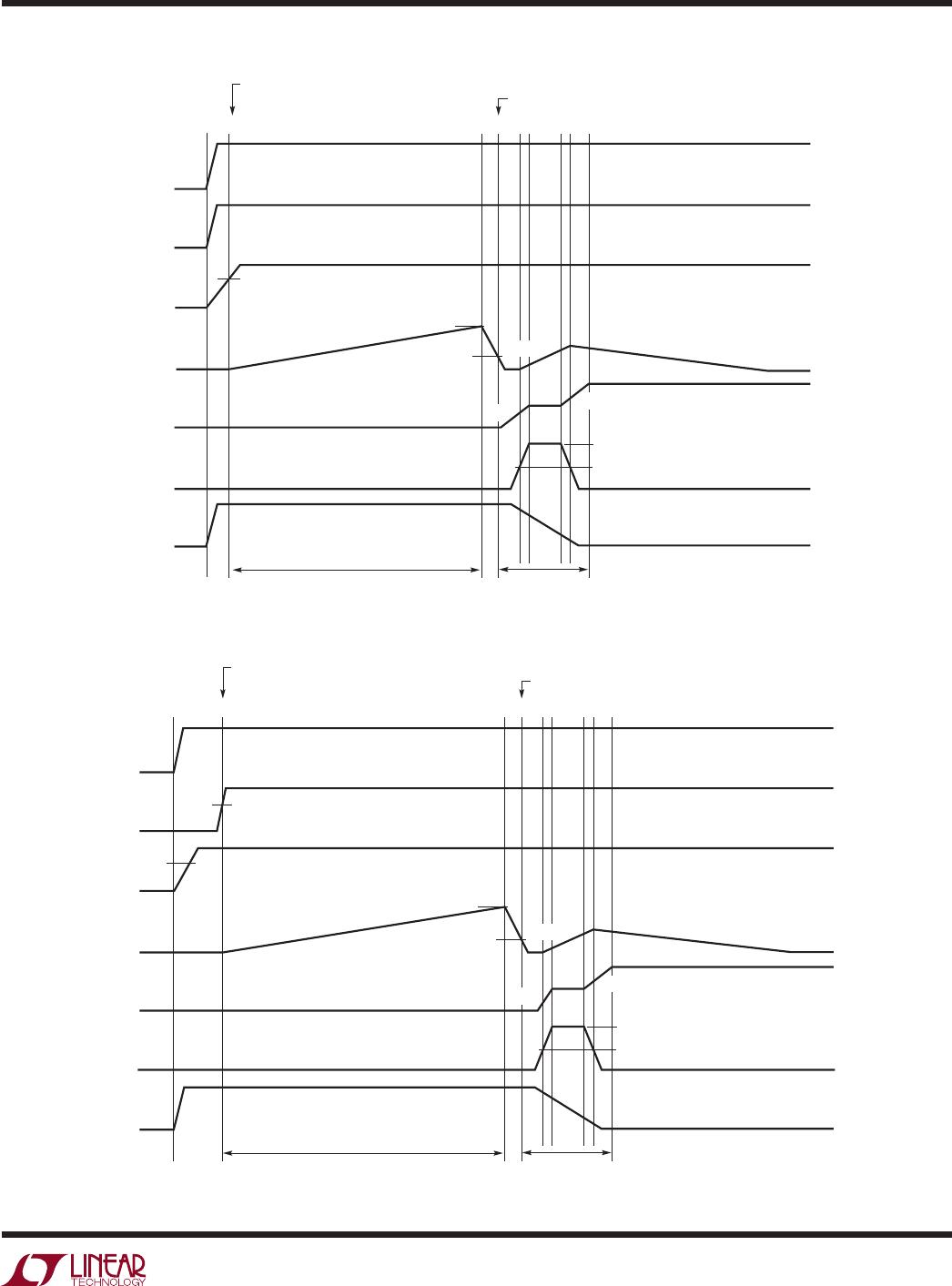
Live Insertion with Short Pin Control of UV/OV
In this example as shown in Figure 8, power is delivered
through long connector pins whereas the UV/OV divider
makes contact through a short pin. This ensures the power
connections are firmly established before the LTC4251/
LTC4251-1/LTC4251-2 are activated. At time point 1, the
power pins make contact and V
IN
ramps through V
LKO
.
At time point 2, the UV/OV divider makes contact and
its voltage exceeds V
UVHI
. In addition, the internal logic
checks for V
UVHI
< UV/OV < V
OVHI
, TIMER < V
TMRL
, GATE
< V
GATEL
and SENSE < V
CB
. When all conditions are met,
an initial timing cycle starts and the TIMER capacitor
is charged by a 5.8µA current source pull-up. At time
point 3, TIMER reaches the V
TMRH
threshold and the ini-
tial timing cycle terminates. The TIMER capacitor is then
quickly discharged. At time point 4, the V
TMRL
threshold
is reached and the conditions of GATE < V
GATEL
and
SENSE < V
CB
must be satisfied before a start-up cycle is
allowed to begin. GATE sources 58µA into the external
MOSFET gate and compensation network. When the
GATE voltage reaches the MOSFET’s threshold, current
begins flowing into the load capacitor. At time point 5, the
SENSE voltage (V
SENSE
– V
EE
) reaches the V
CB
threshold
and activates the TIMER. The TIMER capacitor is charged
by a 230µA current source pull-up. At time point 6, the
analog current limit loop activates. Between time point
6 and time point 7, the GATE voltage is held essentially
constant and the sense voltage is regulated at V
ACL
. As
the load capacitor nears full charge, its current begins to
APPLICATIONS INFORMATION
decline. At time point 7, the load current falls and the sense
voltage drops below V
ACL
. The analog current limit loop
shuts off and the GATE pin ramps further. At time point
8, the sense voltage drops below V
CB
and TIMER now
discharges through a 5.8µA current source pull-down.
At time point 9, GATE reaches its maximum voltage as
determined by V
IN
.
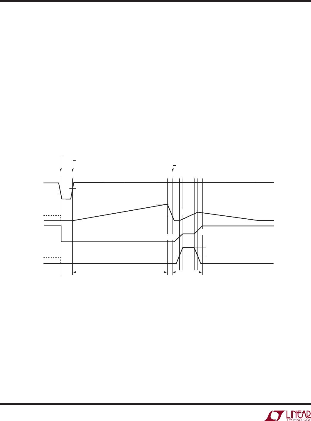
Undervoltage Lockout Timing
In Figure 9, when UV/OV drops below V
UVLO
(time point 1),
TIMER and GATE pull low. If current has been flowing, the
SENSE pin voltage decreases to zero as GATE collapses.
When UV/OV recovers and clears V
UVHI
(time point 2),
an initial time cycle begins followed by a start-up cycle.
Undervoltage Timing with Overvoltage Glitch
In Figure 10, when UV/OV clears V
UVHI
(time point 1),
an initial timing cycle starts. If the system bus voltage
overshoots V
OVHI
as shown at time point 2, TIMER dis-
charges. At time point 3, the supply voltage recovers and
drops below the V
OVLO
threshold. The initial timing cycle
restarts followed by a start-up cycle.
Overvoltage Timing
During normal operation, if UV/OV exceeds V
OVHI
as
shown at time point 1 of Figure 11, the TIMER status is
unaffected. Nevertheless, GATE pulls down and discon-
nects the load. At time point 2, UV/OV recovers and drops
below the V
OVLO
threshold. A gate ramp up cycle ensues.
If the overvoltage glitch is long enough to deplete the
load capacitor, a full start-up cycle may occur as shown
between time points 3 through 6.
Timer Behavior
In Figure 12a, the TIMER capacitor charges at 230µA if
the SENSE pin exceeds V
CB
. It is discharged with 5.8µA
if the SENSE pin is less than V
CB
. In Figure 12b, when
TIMER exceeds V
TMRH
, TIMER is latched high by the 5.8µA
pull-up and GATE pulls down immediately. In Figure 12c,
multiple momentary faults cause the TIMER capacitor to
integrate until it latches.