7
425112fd
LTC4251/LTC4251-1/
LTC4251-2
For more information www.linear.com/4251
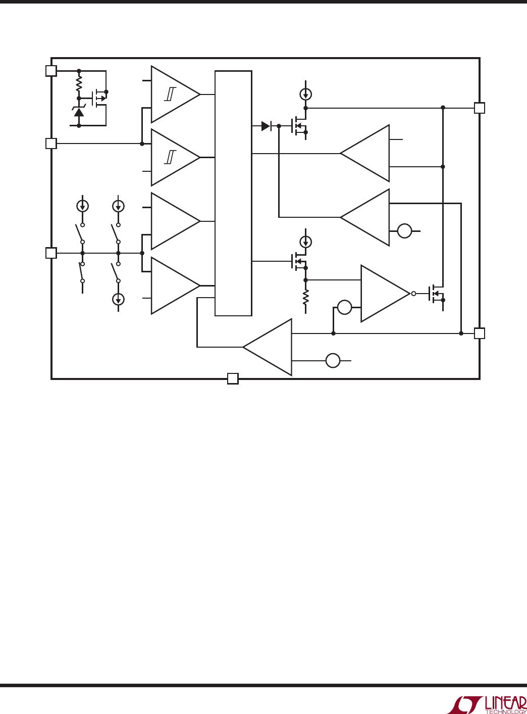
PIN FUNCTIONS
SENSE (Pin 1): Circuit Breaker/Current Limit SENSE Pin.
Load current is monitored by sense resistor R
S
connected
between SENSE and V
EE
, and controlled in three steps. If
SENSE exceeds V
CB
(50mV), the circuit breaker comparator
activates a 230µA TIMER pin pull-up current. The LTC4251/
LTC4251-1/LTC4251-2 latch off when C
T
charges to 4V. If
SENSE exceeds V
ACL
(100mV), the analog current limit
amplifier pulls GATE down and regulates the MOSFET
current at V
ACL
/R
S
. In the event of a catastrophic short-
circuit, SENSE may overshoot 100mV. If SENSE reaches
V
FCL
(200mV), the fast current limit comparator pulls
GATE low with a strong pull-down. To disable the circuit
breaker and current limit functions, connect SENSE to V
EE
.
Kelvin-sense connections between the sense resistor and
the V
EE
and SENSE pins are strongly recommended, see
Figure 6.
V
EE
(Pin 2): Negative Supply Voltage Input. Connect this
pin to the negative side of the power supply.
V
IN
(Pin 3): Positive Supply Input. Connect this pin to the
positive side of the supply through a dropping resistor.
A shunt regulator typically clamps V
IN
at 13V. An internal
undervoltage lockout (UVLO) circuit holds GATE low until
the V
IN
pin is greater than V
LKO
(9.2V), overriding UV/OV. If
UV is high, OV is low and V
IN
comes out of UVLO, TIMER
starts an initial timing cycle before initiating a GATE ramp
up. If V
IN
drops below approximately 8.2V, GATE pulls low
immediately.
TIMER (Pin 4): Timer Input. TIMER is used to generate
a delay at start-up, and to delay shutdown in the event of
an output overload. TIMER starts an initial timing cycle
when the following conditions are met: UV is high, OV is
low, V
IN
clears UVLO, TIMER pin is low, GATE is lower than
V
GATEL
and V
SENSE
– V
EE
< V
CB
. A pull-up current of 5.8µA
then charges C
T
, generating a time delay. If C
T
charges to
V
TMRH
(4V) the timing cycle terminates, TIMER quickly
pulls low and GATE is activated.
If SENSE exceeds 50mV while GATE is high, a 230µA
pull-up current charges C
T
. If SENSE drops below 50mV
before TIMER reaches 4V, a 5.8µA pull-down current
slowly discharges C
T
. In the event that C
T
eventually
integrates up to the 4V V
TMRH
threshold, TIMER latches
high with a 5.8µA pull-up source and GATE quickly pulls
low. The LTC4251/LTC4251-1/LTC4251-2 fault latches may
be cleared by either pulling TIMER low with an external
device, or by pulling UV/OV below V
UVLO
.
UV/OV (Pin 5): Undervoltage/Overvoltage Input. This dual
function pin detects undervoltage as well as overvoltage.
The high threshold at the UV comparator is set at V
UVHI
with V
UVHST
hysteresis. The high threshold at the OV
comparator is set at V
OVHI
with V
OVHST
hysteresis. If UV/
OV < V
UVLO
or UV/OV > V
OVHI
, GATE pulls low. If UV/OV
> V
UVHI
and UV/OV < V
OVLO
, the LTC4251/LTC4251-1/
LTC4251-2 attempt to start-up. The internal UVLO at V
IN
always overrides UV/OV. A low at UV resets an internal fault
latch. A high at OV pulls GATE low but does not reset the
fault latch. A 1nF to 10nF capacitor at UV/OV eliminates
transients and switching noise from affecting the UV/OV
thresholds and prevents glitches at the GATE pin.
GATE (Pin 6): N-Channel MOSFET Gate Drive Output.
This pin is pulled high by a 58µA current source. GATE is
pulled low by invalid conditions at V
IN
(UVLO), UV/OV, or
the fault latch. GATE is actively servoed to control fault
current as measured at SENSE. A compensation capacitor
at GATE stabilizes this loop. A comparator monitors GATE
to ensure that it is low before allowing an initial timing
cycle, GATE ramp up after an overvoltage event, or restart
after a current limit fault.
UV/OV refers to the UV pin for the LTC4251-2. The OV comparator in the LTC4251-2 is disabled. All
references in the text to overvoltage, OV, V
OVHI
and V
OVLO
do not apply to the LTC4251-2.