IDT
TM
/ICS
TM
DDR I/DDR II Phase Lock Loop Zero Delay Buffer ICS9P935 REV H 12/1/08
ICS9P935
DDR I/DDR II Phase Lock Loop Zero Delay Buffer
2
Pin Description
Pin# Pin Name Type Pin Description
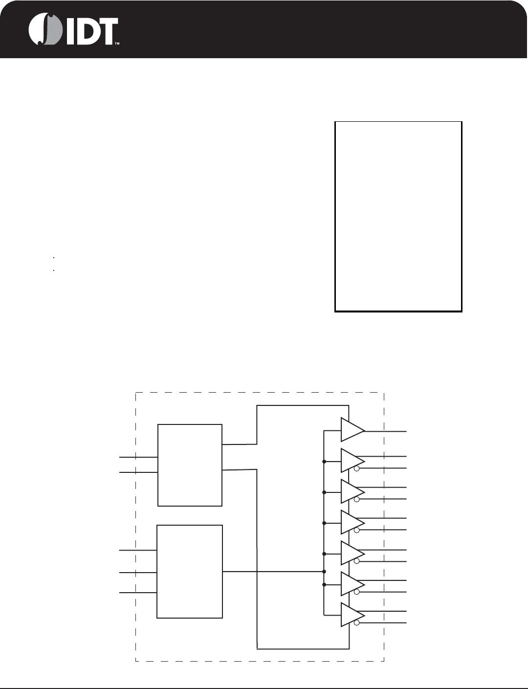
1 DDRC0 OUT "Complementary" Clock of differential pair output.
2 DDRT0 OUT "True" Clock of differential pair output.
3 VDD2.5/1.8 PWR Power supply, nominal 2.5V or 1.8V
4 DDRT1 OUT "True" Clock of differential pair output.
5 DDRC1 OUT "Complementary" Clock of differential pair output.
6 GND PWR Ground pin.
7 VDDA2.5/1.8 PWR Output power supply, nominal 2.5V or 1.8V
8 GND PWR Ground pin.
9 CLK_INT IN "True" reference clock input.
10 CLK_INC IN "Complementary" reference clock input.
11 VDD2.5/1.8 PWR Power supply, nominal 2.5V or 1.8V
12 DDRT2 OUT "True" Clock of differential pair output.
13 DDRC2 OUT "Complementary" Clock of differential pair output.
14 GND PWR Ground pin.
15 DDRC3 OUT "Complementary" Clock of differential pair output.
16 DDRT3 OUT "True" Clock of differential pair output.
17 FB_OUT OUT Feedback output, dedicated for external feedback.
18 FB_IN IN
Single-ended feedback input, provides feedback signal to internal PLL to eliminate
phase error with the input clock.
19 SCLK IN Clock pin of SMBus circuitry, 3.3V tolerant.
20 SDATA I/O Data pin for SMBus circuitry, 3.3V tolerant.
21 VDD2.5/1.8 PWR Power supply, nominal 2.5V or 1.8V
22 DDRT4 OUT "True" Clock of differential pair output.
23 DDRC4 OUT "Complementary" Clock of differential pair output.
24 GND PWR Ground pin.
25 VDD2.5/1.8 PWR Power supply, nominal 2.5V or 1.8V
26 DDRT5 OUT "True" Clock of differential pair output.
27 DDRC5 OUT "Complementary" Clock of differential pair output.
28 GND PWR Ground pin.