IDT
TM
/ICS
TM
DDR I/DDR II Phase Lock Loop Zero Delay Buffer ICS9P935 REV H 12/1/08
ICS9P935
DDR I/DDR II Phase Lock Loop Zero Delay Buffer
4
Notes:
1. Unused inputs must be held high or low to prevent them from floating.
2. DC input signal voltage specifies the allowable DC execution of differential input.
3. Differential inputs signal voltages specifies the differential voltage [VTR-VCP] required
for switching, where VTR is the true input level and VCP is the complementary input
level.
4. Differential cross-point voltage is expected to track variations of V
DD
and is the voltage
at which the differential signal must be crossing.
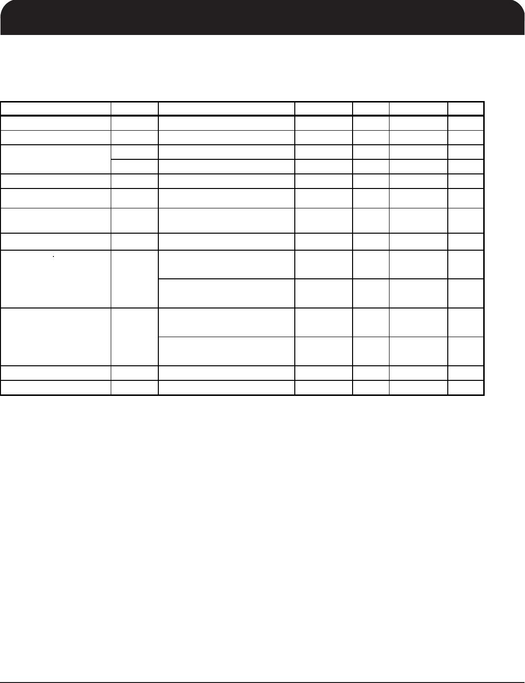
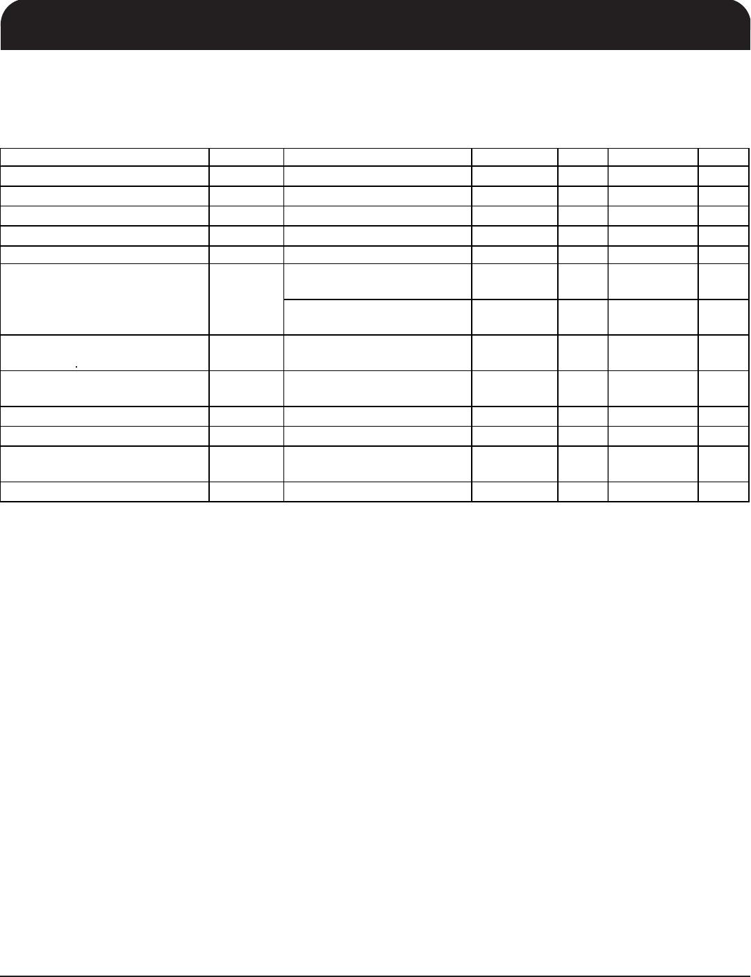
Recommended Operating Condition
see note1
T
A
= 0 - 70°C; Supply Voltage AVDD, VDD = 1.8 V +/- 0.1V (unless otherwise stated)
PARAMETER SYMBOL CONDITIONS MIN TYP MAX UNITS
Supply Voltage V
DDQ
, A
VD
1.7 1.8 1.9 V
Low level input voltage V
IL
CLK_INT, CLK_INC, FB_IN 0.35 x V
D
V
High level input voltage V
IH
CLK_INT, CLK_INC, FB_IN 0.65 x V
DD
V
DC input signal voltage (note 2) V
IN
-0.3 V
DD
+ 0.3 V
DC input si
nal volta
e swin
V
IN-Diff
CLK_INT, CLK_INC GND - 0.3
1.5 V
D
+ 0.3 V
DC - CLK_INT, CLK_INC,
FB_IN
0.3 V
DD
+ 0.4 V
AC - CLK_INT, CLK_INC,
FB_IN
0.6 V
DD
+ 0.4 V
Output differential cross-voltage
(note 4)
V
OX
V
DD
/ 2 - 0.1 V
DD
/ 2 + 0.1 V
Input differential cross-voltage
(note 4)
V
IX
V
DD
/2 - 0.15 V
DD
/2 V
DD
/ 2 + 0.15 V
High level output current I
OH
-9 mA
Low level output current I
OL
9mA
High Impedance
Output Current
I
OZ
V
DD
=1.9V, V
OUT
=V
DD
or GND
±
10 mA
Operating free-air temperature T
A
070°C
Differential input signal voltage
(note 3)
V
ID