IDT
TM
/ICS
TM
DDR I/DDR II Phase Lock Loop Zero Delay Buffer ICS9P935 REV H 12/1/08
ICS9P935
DDR I/DDR II Phase Lock Loop Zero Delay Buffer
7
Recommended Operating Condition (see note 1)
Notes:
1. Unused inputs must be held high or low to prevent them from floating.
2. DC input signal voltage specifies the allowable DC execution of differential input.
3. Differential inputs signal voltages specifies the differential voltage [VTR-VCP] required
for switching, where VT is the true input level and VCP is the complementary input level.
4. Differential cross-point voltage is expected to track variations of V
DD
and is the voltage
at which the differential signal must be crossing.
T
A
= 0 - 70°C; Supply Voltage AVDD, VDD = 2.5 V +/- 0.2V (unless otherwise stated)
PARAMETER SYMBOL CONDITIONS MIN TYP MAX UNITS
Supply Voltage V
DD
, A
VDD
2.3 2.5 2.7 V
DDRT,DDRC 0.4 V
DD
/2 - 0.18 V
DDRT,DDRC V
DD
/2 + 0.18 2.1 V
DC input signal voltage
(note 2)
V
IN
-0.3 V
DD
+ 0.3 V
DC - DDRT 0.36 V
DD
+ 0.6 V
AC - DDRT 0.7 V
DD
+ 0.6 V
Output differential cross
-
volta
g
e (note 4)
V
OX
V
DD
/2 - 0.15 V
DD
/2 + 0.15 V
Input differential cross-
volta
g
e (note 4)
V
IX
V
DD
/2 - 0.2 V
DD
/2 V
DD
/2 + 0.2 V
High level output
current
I
OH
-30 mA
Low level output current I
OL
-30 mA
Operating free-air
temperature
T
A
085°C
Differential input signal
voltage (note 3)
V
ID
Low level input voltage
V
IL
High level input voltage
V
IH
IDT
TM
/ICS
TM
DDR I/DDR II Phase Lock Loop Zero Delay Buffer ICS9P935 REV H 12/1/08
ICS9P935
DDR I/DDR II Phase Lock Loop Zero Delay Buffer
8
Timing Requirements
Switching Characteristics
3
Notes:
1. Refers to transition on noninverting output in PLL bypass mode.
2. While the pulse skew is almost constant over frequency, the duty cycle error increases at
higher frequencies. This is due to the formula: duty cycle=t
wH
/t
c
, were the cycle (t
c
)
decreases as the frequency goes up.
3. Switching characteristics guaranteed for application frequency range.
4. Static phase offset shifted by design.
T
A
= 0 - =70°C; Supply Voltage A
VDD
, V
DD
= 2.5 V +/- 0.2V (unless otherwise stated)
PARAMETER SYMBOL
CONDITIONS
MIN MAX UNITS
Max clock frequency freq
op
2.5V+0.2V @ 25
o
C
45 600 MHz
Application Frequency
Range
freq
App
2.5V+0.2V @ 25
o
C
95 233 MHz
Input clock duty cycle d
tin
40 60 %
CLK stabilization T
STAB
15 µs
PARAMETER SYMBOL CONDITION MIN TYP MAX UNITS
Low-to high level
propagation delay time
t
PLH
1
BUF_IN to any output 3.5 ns
High-to low level propagation
delay time
t
PLL
1
BUF_IN to any output 3.5 ns
Period jitter T
j
it
(p
er
)
100MHz to 200MHz -30 30 ps
Half-period jitter t(jit_hper) 100MHz to 200MHz -100 100 ps
Input clock slew rate t
sl
(
i
)
14V/ns
Output clock slew rate t
sl
(
o
)
12V/ns
Cycle to Cycle Jitter
1
T
c
y
c
-T
c
y
c
100MHz to 200MHz -50 50 ps
Static Phase Offset
t
(
static
p
hase offset
)
4
-50 0 50 ps
Output to Output Skew T
skew
40 ps
IDT
TM
/ICS
TM
DDR I/DDR II Phase Lock Loop Zero Delay Buffer ICS9P935 REV H 12/1/08
ICS9P935
DDR I/DDR II Phase Lock Loop Zero Delay Buffer
9
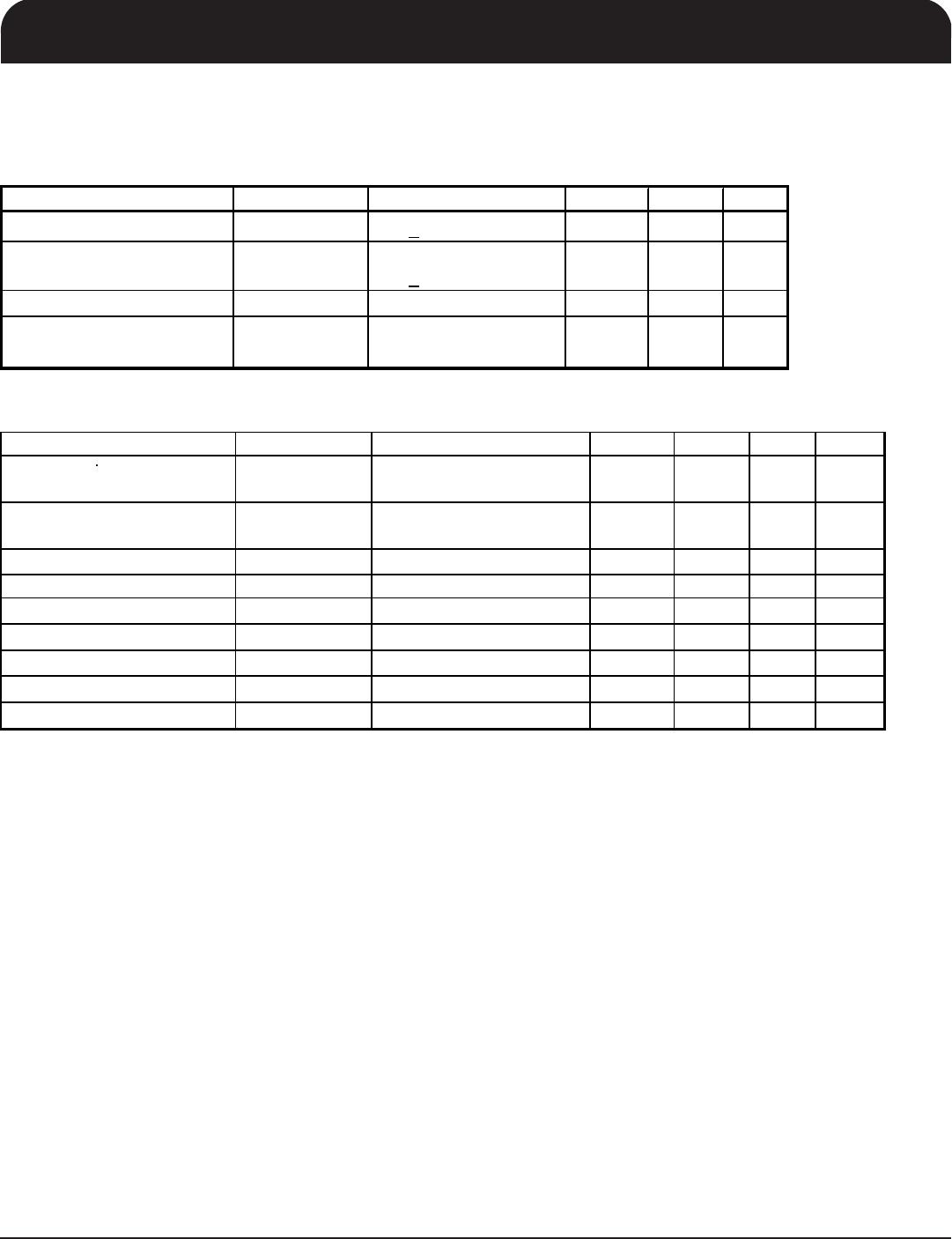
1. The IDT clock generator is a slave/receiver, I
2
C component. It can read back the data stored in the latches for verification.
Read-Back will support SMBus block read protocol.
2. The data transfer rate supported by this clock generator is 100K bits/sec or less (standard mode)
3. The input is operating at 3.3V logic levels.
4. The data byte format is 8 bit bytes.
5. To simplify the clock generator I
2
C interface, the protocol is set to use only "Block-Writes" from the controller. The bytes must
be accessed in sequential order from lowest to highest byte with the ability to stop after any complete byte has been transferred.
The Command code and Byte count shown above must be sent, The data is loaded until a Stop sequence is issued.
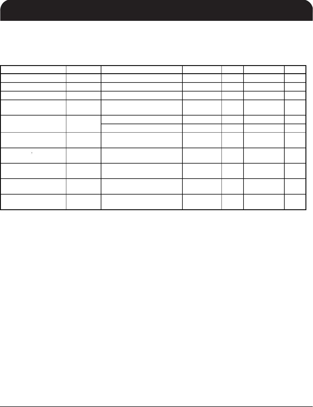
6. At power-on, all registers are set to a default condition, as shown.
Notes:
General I
2
C serial interface information for the ICS9P935
How to Write:
Controller (host) sends a start bit.
Controller (host) sends the write address D4
(H)
ICS clock will
acknowledge
Controller (host) sends the begining byte location = N
ICS clock will
acknowledge
Controller (host) sends the data byte count = X
ICS clock will
acknowledge
Controller (host) starts sending
Byte N through
Byte N + X -1
(see Note 2)
ICS clock will
acknowledge
each byte
one at a time
Controller (host) sends a Stop bit
How to Read:
Controller (host) will send start bit.
Controller (host) sends the write address D4
(H)
ICS clock will
acknowledge
Controller (host) sends the begining byte
location = N
ICS clock will
acknowledge
Controller (host) will send a separate start bit.
Controller (host) sends the read address D5
(H)
ICS clock will
acknowledge
ICS clock will send the data byte count = X
ICS clock sends
Byte N + X -1
ICS clock sends
Byte 0 through byte X (if X
(H)
was written to byte 8)
.
Controller (host) will need to acknowledge each byte
Controllor (host) will send a not acknowledge bit
Controller (host) will send a stop bit
ICS (Slave/Receiver)
T
WR
ACK
ACK
ACK
ACK
ACK
P
Byte N + X - 1
Data Byte Count = X
Beginning Byte N
stoP bit
X Byte
Index Block Write Operation
Slave Address D4
(H)
Beginning Byte = N
WRite
starT bit
Controller (Host)
TstarT bit
WR WRite
RT Repeat starT
RD ReaD
Beginning Byte N
Byte N + X - 1
N Not acknowledge
PstoP bit
ICS (Slave/Receiver)
Controller (Host)
X Byte
ACK
ACK
Data Byte Count = X
ACK
Slave Address D5
(H)
Index Block Read Operation
Slave Address D4
(H)
Beginning Byte = N
ACK
ACK

9P935AFLFT

Mfr. #:
Manufacturer:
IDT
Description:
Clock Buffer PC BUFFER
Lifecycle:
New from this manufacturer.
Delivery:
DHL FedEx Ups TNT EMS
Payment:
T/T Paypal Visa MoneyGram Western Union

Products related to this Datasheet