LT3782A
13
3782afc
For more information www.linear.com/LT3782A
For a given V
IN
and V
OUT
, we can calculate the duty cycle D
and then derive the output RMS ripple current from Figure 6.
After choosing
output capacitors with sufficient RMS
ripple current rating, we also need to consider the ESR
requirement if electrolytic caps, tantalum caps, POSCAPs
or SP CAPs are selected. Given the required output ripple
voltage specV
OUT
(in RMS value) and the calculated RMS
ripple currentI
OUT
, one can estimate the ESR value of
the output capacitor to be
ESR
Δ
V
OUT
ΔI
OUT
External Regulator to Bias Gate Drivers
For applications with V
IN
higher than 24V, the IC tempera-
ture may get too high. To reduce heat, an external regulator
between 12V to 14V should be used to override the internal
V
GBIAS
regulator to supply the current needed for BGATE1
and BGATE2 (see Figure 7).
Efficiency Considerations
The efficiency of a switching regulator is equal to the out
-
put power divided by the input power (¥100%). Percent
efficiency can be expressed as:
% Efficiency = 100% – (L1 + L2 + L3 + …),
where L1, L2, etc. are the individual loss components
as a percentage of the input power. It is often useful to
analyze individual losses to determine what is limiting
the efficiency and which change would produce the most
improvement. Although all dissipative elements in the
circuit produce losses, four main sources usually account
for the majority of the losses in LT3782A application
circuits:
1.
The supply current into V
IN
. The V
IN
current is the sum
of the DC supply current I
Q
(given in the Electrical Char-
acteristics) and the
MOSFET driver and control currents.
The DC supply current into the V
IN
pin is typically about
7mA and represents a small power loss (much less
than 1%) that
increases with V
IN
. The driver current
results from switching the gate capacitance of the power
MOSFET; this current is typically much larger than the
DC current. Each time the MOSFET is switched on and
then off, a packet of gate charge Q
G
is transferred from
GBIAS to ground. The resulting dQ/dt is a current that
must be supplied to the GBIAS capacitor through the
V
IN
pin by an external supply. In normal operation:
I
Q(TOT)
≈ I
Q
= fQ
G
P
IC
= V
IN
• (I
Q
+ fQ
G
)
2. Power MOSFET switching and conduction losses:
P
FET
=
I
O(MAX)
2
1 D
MAX
2
R
DS(ON)
D
MAX
ρ
T
+ k V
O
2
I
O(MAX)
2
1 D
MAX
C
RSS
f
Figure 7
3782A F07
2µF
12V
+
GBIAS
GBIAS1
GBIAS2
LT3782A
applicaTions inForMaTion
LT3782A
14
3782afc
For more information www.linear.com/LT3782A
3. The I
2
R losses in the sense resistor can be calculated
almost by inspection:
P
R(SENSE)
=
I
O(MAX)
2
1 D
MAX
2
R D
MAX
4. The losses in the inductor are simply the DC input cur-
rent squared times the winding resistance. Expressing
this loss as a function of the output current yields:
P
R(WINDING)
=
I
O(MAX)
2
1 D
MAX
2
R
W
5. Losses in the boost diode. The power dissipation in the
boost diode is:
P
DIODE
=
I
O(MAX)
2
V
D
The boost diode can be a major source of power loss
in a boost converter. For 13.2V input, 42V output at 3A,
a Schottky diode with a 0.4V forward voltage would
dissipate 600mW, which represents about 1% of the
input power. Diode losses can become significant at
low output voltages where the forward voltage is a
significant percentage of the output voltage.
6. Other losses, including C
IN
and C
O
ESR dissipation and
inductor core losses, generally account for less than
2% of the total losses.
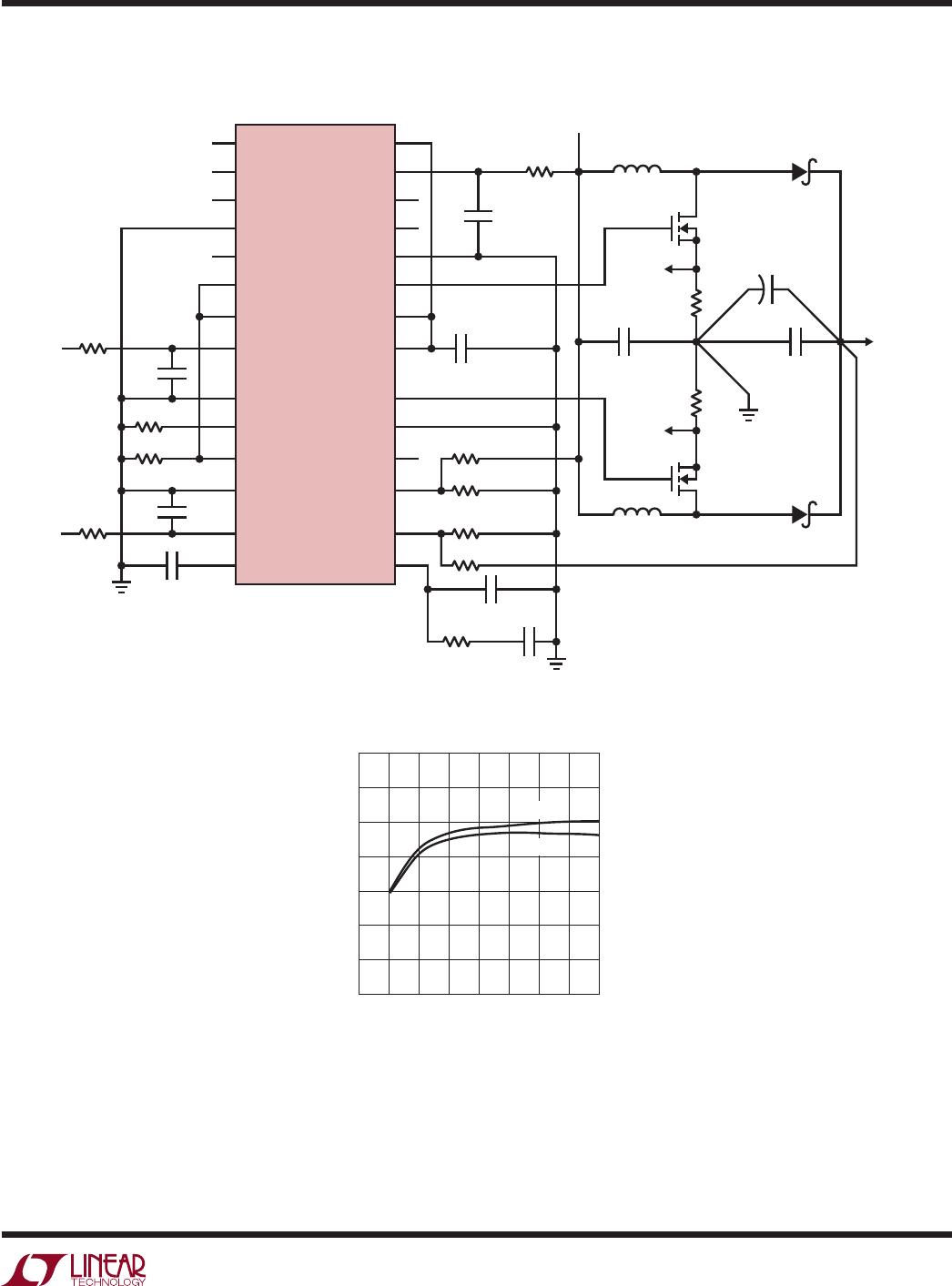
PCB Layout Considerations
To achieve best performance from an LT3782A circuit,
the PC board layout must be carefully done. For lower
power applications, a two-layer PC board is sufficient.
However, at higher power levels, a multiplayer PC board
is recommended. Using a solid ground plane under the
circuit is the easiest way to ensure that switching noise
does not affect the operation.
In order to help dissipate the power from MOSFETs and
diodes, keep the ground plane on the layers closest to the
layers where power components are mounted. Use power
planes for MOSFETs and diodes in order to improve the
spreading of the heat from these components into the PCB.
For best
electrical performance, the LT3782A circuit should
be laid out as follows:
Place all power components in a tight area. This will
minimize the size of high current loops. Orient the input
and output capacitors and current sense resistors in a way
that minimizes the distance between the pads connected
to ground plane.
Place the LT3782A and associated components tightly
together and next to the section with power components.
Use a local via to ground plane for all pads that connect to
ground. Use multiple vias for power components.
Connect the current sense inputs of LT3782A directly
to the current sense resistor pads. Connect the current
sense traces on the opposite sides of pads from the traces
carrying the MOSFETs source currents to ground. This
technique is referred to as Kelvin sensing.
applicaTions inForMaTion
LT3782A
15
3782afc
For more information www.linear.com/LT3782A
I
OUT
(A)
0
EFFICIENCY (%)
100
96
98
94
92
90
88
86
7
3782A TA02b
1 2 4 6
3
5
8
12V
IN
15V
IN
Efficiency
10Ω
CS2
C
OUT2
330µF, 35V, ×2
+
27
26
25
24
23
22
21
20
19
18
17
16
15
28
2
3
4
5
6
7
8
9
10
11
12
13
14
1
10Ω
CS1
59k
82k
274k
825k
2R2
24.9k
221k
R
C1
13.3k
10nF
4.7nF
C
C2
100pF
C
C1
6.8nF
2.2µF
C
IN
22µF
25V
C
OUT1
22µF, 25V, ×4
10nF
1µF
3782A TA02
10V TO 24V INPUT
Q1
PH3330
Q2
PH3330
OUTPUT
24V
8A
L1, L2: PULSE PB2020-103
ALL CERAMIC CAPACITORS ARE X7R, TDK
*OUTPUT CURRENT WITH BOTH INPUTS PRESENT
L1
PB2020-103
D1
PDS1040
L2
PB2020-103
D2
PDS1040
CS1
CS2
0.004Ω
0.004Ω
LT3782A
V
CC
NC
NC
V
EE1
BGATE1
GBIAS1
GBIAS2
BGATE2
V
EE2
NC
RUN
FB
V
C
GBIAS
SGATE1
NC
GND
SYNC
DELAY
DCL
SENSE1
+
SENSE1
SLOPE
R
SET
SENSE2
SENSE2
+
SS
SGATE2
10V to 24V Input to 24V, 8A Output Boost Converter
Typical applicaTions

LT3782AEFE#PBF

Mfr. #:
Manufacturer:
Analog Devices / Linear Technology
Description:
Switching Voltage Regulators 2-PhBoost DC/DC Cntr
Lifecycle:
New from this manufacturer.
Delivery:
DHL FedEx Ups TNT EMS
Payment:
T/T Paypal Visa MoneyGram Western Union