LT3782A
4
3782afc
For more information www.linear.com/LT3782A
V
CC
(V)
6
I
CC
(mA)
20
18
16
12
14
10
8
6
4
2
0
22
3782A G02
108 12 16 20 26
14
18
30
24
28
V
CC
(V)
6
∆V
REF
(mV)
30
3782A G03
12
18
24
27
9
15
21
3
2
1
0
–1
–2
–3
–4
–5
∆FREQUENCY (kHz)
12
10
8
6
4
2
0
–2
–4
∆FREQUENCY
∆V
REF
I
GBIAS
(mA)
0
V
GBIAS
(V)
10.5
100
3782A G01
10.0
10.6
10.1
10.7
10.2
10.8
10.3
10.9
10.4
50
11.0
The l denotes the specifications which apply over the full operating junction
temperature range, otherwise specifications are at T
J
= 25°C. V
CC
= 13V, R
SET
= 80k, no load on any outputs, unless otherwise noted.
Note 1: Stresses beyond those listed under Absolute Maximum Ratings
may cause permanent damage to the device. Exposure to any Absolute
Maximum Rating condition for extended periods may affect device
reliability and lifetime.
Note 2: The LT3782AE is guaranteed to meet performance specifications
from 0°C to 85°C operating junction temperature. Specifications over
the –40°C to 125°C operating junction temperature range are assured by
design, characterization and correlation with statistical process controls.
The LT3782AI is guaranteed to meet performance specifications over the
full –40°C to 125°C operating junction temperature range. The maximum
ambient temperature is determined by specific operating conditions in
conjunction with board layout, the rated package thermal resistance and
other environmental factors.
Note 3: This IC includes overtemperature protection that is intended
to protect the device during momentary overload conditions. Junction
temperature will exceed 125°C when overtemperature protection is active.
Continuous operation above the specified maximum operating junction
temperature may impair device reliability.
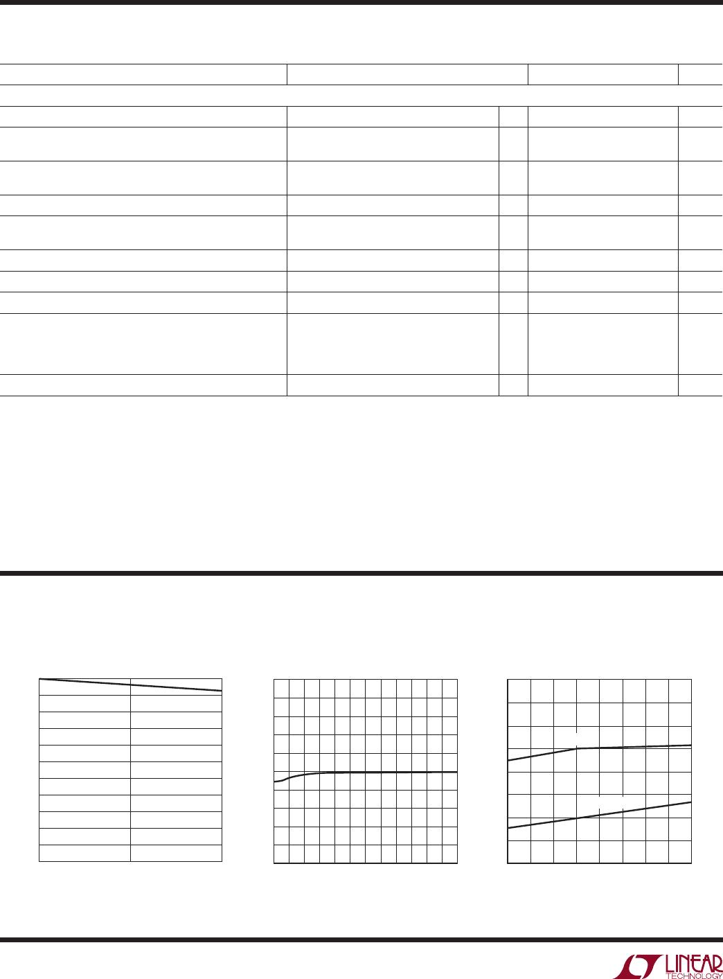
V
GBIAS
vs I
GBIAS
I
CC
vs V
CC
∆V
REF
vs V
CC
, ∆Frequency vs V
CC
(R
SET
= 80k)
elecTrical characTerisTics
PARAMETER CONDITIONS MIN TYP MAX UNITS
Gate Driver
V
GBIAS
I
GBIAS
< 70mA
l
10.2 11 11.7 V
BGATE1, BGATE2 High Voltage 13V ≤ V
CC
≤ 24V, I
BGATE
= –100mA
V
CC
= 8V, I
BGATE
= –100mA
l
l
7.8
3.8
9.2
5
10.5 V
V
BGATE1, BGA
TE2 Source Current (Peak) Capacitive Load >22µF
Capacitive Load >50µF
3
4
A
A
BGATE1, BGA
TE2 Low Voltage 8V ≤ V
CC
≤ 24V, I
BGATE
= 100mA
l
0.5 0.7 V
BGATE1, BGATE2 Sink Current (Peak) Capacitive Load >22µF
Capacitive Load >50µF
3
4
A
A
SGATE1, SGA
TE2 High Voltage 8V ≤ V
CC
≤ 24V, I
SGATE
= –20mA
l
4.5 5.5 6.7 V
SGATE1, SGATE2 Low Voltage 8V ≤ V
CC
≤ 24V, I
SGATE
= 20mA 0.5 0.7 V
SGATE1, SGATE2 Peak Current 500pF Load 100 mA
Delay of BGATE High DELAY Pin and R
SET
Pin Shorted
V
DELAY
= 1V
V
DELAY
= 0.5V
V
DELAY
= 0.25V
100
150
250
500
ns
ns
ns
ns
Delay Pin Input Current V
DELAY
= 0.25V
l
–0.1 –0.3 µA
T
J
= 25°C unless otherwise noted.
Typical perForMance characTerisTics
LT3782A
5
3782afc
For more information www.linear.com/LT3782A
R
FREQ
(kΩ)
0
FREQUENCY (kHz)
600
500
400
300
200
100
160
3782A G04
4020 60 100 140
80
120
200
180
TIME (s)
0
V
GBIAS
(V)
14
10
6
2
12
8
4
0
–2
I
GBIAS
(mA)
800
600
400
200
700
500
300
100
0
750µ
3782A G06
250µ 500µ
1m
V
GBIAS
I
GBIAS
V
DELAY
(V)
0
DELAY (ns)
1000
900
800
600
700
500
400
300
200
100
0
2.0
3782A G07
0.5
1.0
1.5
2.5
SWITCHING FREQUENCY (kHz)
100
DUTY CYCLE (%)
105
100
95
90
85
80
500
3782A G08
200
300
400
600
V
DCL
(V)
0
MAXIMUM DUTY CYCLE (%)
2.4
3782A G09
0.6
1.2
1.8
2.1
0.3
0.9
1.5
120
110
100
90
80
70
60
50
40
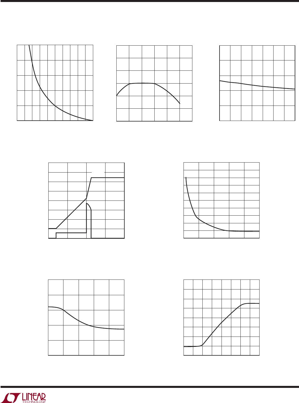
Switching Frequency vs R
FREQ
Reference Voltage
vs Temperature
V
GBIAS
vs I
GBIAS
at Start-Up
(Charging 2µF)
SGATE (Low) to BGATE (High)
Delay vs V
DELAY
(R
SET
= 80k)
Switching Frequency
vs Duty Cycle
Maximum Duty Cycle Limit
vs V
DCL
(R
SET
= 80k)
T
J
= 25°C, unless otherwise noted.
Typical perForMance characTerisTics
TEMPERATURE (°C)
–45
CURRENT LIMIT THRESHOLD (mV)
3782A G10
5
55
105
130
–20
30
80
70
67
64
61
58
55
Current Limit Threshold
vs Temperature
LT3782A
6
3782afc
For more information www.linear.com/LT3782A
SGATE2 (Pin 1/Pin 26): Second Phase Synchronous Drive
Signal. An external driver buffer is needed to drive the top
synchronous power FET.
SGATE1 (Pin 2/Pin 27): First Phase Synchronous Drive
Signal. An external driver buffer is needed to drive the top
synchronous power FET.
GND (Pin 4, Exposed Pad Pin 29/Pin 28, Exposed Pad
Pin 29): Ground.
Solder the exposed pad to the PCB
ground plane for rated thermal performance. The exposed
pad should be connected to the GND pin as close to the
IC as possible.
SYNC (Pin 5/Pin 1): Synchronization Input. The pulse
width can range from 10% to 70%. Note that the operating
frequency is half of the sync frequency.
DELAY (Pin 6/Pin 2): When synchronous drivers are used,
the programmable delay that delays BGATE turns on after
SGATE turns off.
DCL (Pin 7/Pin 3): This pin programs the limit of the
maximum duty cycle. When connected to V
RSET
, it oper-
ates at natural maximum duty cycle, approximately 90%.
SENSE
1
+
(Pin 8/Pin 4): First Phase Current Sense Amplifier
Positive Input. An RC filter is required across the current
sense resistor. Current limit threshold is set at 63mV.
SENSE1
(Pin 9/Pin 5): First Phase Current Sense Ampli-
fier Negative Input.
SLOPE (
Pin 10/Pin 6): A resistor from SLOPE to GND
increases
the internal current mode PWM slope com-
pensation.
R
SET
(Pin 11/Pin 7): A resistor from R
SET
to GND sets the
oscillator charging current and the operating frequency.
SENSE2
(Pin 12/Pin 8): Second Phase Current Sense
Amplifier Negative Input.
SENSE2
+
(Pin 13/Pin 10): Second Phase Current Sense
Amplifier Positive Input. An RC filter is required across
the current sense resistor. Current limit threshold is set
at 63mV.
SS (Pin 14/Pin 11): Soft-Start. A capacitor on this pin sets
the output ramp up rate. The typical time for SS to reach
the programmed level is (C • 2.44V)/10µA.
V
C
(Pin 15/Pin 12): The output of the g
m
error amplifier and
the control signal of the current loop of the current-mode
PWM. Switching starts at 0.7V, and higher V
C
voltages
corresponds to higher inductor current.
FB (Pin 16/Pin 13): Error Amplifier Inverting Input. A
resistor divider to this pin sets the output voltage.
RUN (Pin 17/Pin 14): LT3782A goes into shutdown mode
when V
RUN
is below 2.3V and goes to low bias current
shutdown mode when V
RUN
is below 0.3V.
V
EE2
(Pin 19/Pin 16): Gate Driver BGATE2 Ground. This
pin should be connected
to ground as close to the IC as
possible.
BGATE2 (Pin 20/Pin 17): Second Phase MOSFET Driver.
GBIAS2 (Pin 21/Pin 18): Bias for Gate Driver BGATE2.
Should be connected to GBIAS or an external power supply
between 12V to 14V.
GBIAS1 (Pin 22/Pin 21): Bias for Gate Driver BGATE1.
Should be connected to GBIAS2.
BGATE1 (Pin 23/Pin 22): First Phase MOSFET Driver.
V
EE1
(Pin 24/Pin 23): Gate Driver BGATE1 Ground. This
pin should be connected to ground as close to the IC as
possible.
V
CC
(Pin 27/Pin 24): Chip Power Supply. Good supply
bypassing is required.
GBIAS (Pin 28/Pin 25): Internal 11V regulator output for
biasing internal circuitry. Should be connected to GBIAS1
and GBIAS2. A bypass low ESR capacitor ofF or larger
is needed and should be connected directly to the pin to
minimize parasitic impedance.
NC (Pins 3, 18, 25, 26/Pins 9, 15, 19, 20): Not Connected.
Can be connected to GND.
(FE/UFD)
pin FuncTions
LT3782AEFE#PBF

Mfr. #:
Manufacturer:
Analog Devices / Linear Technology
Description:
Switching Voltage Regulators 2-PhBoost DC/DC Cntr
Lifecycle:
New from this manufacturer.
Delivery:
DHL FedEx Ups TNT EMS
Payment:
T/T Paypal Visa MoneyGram Western Union