For free samples & the latest literature: http://www.maxim-ic.com, or phone 1-800-998-8800.
For small orders, phone 408-737-7600 ext. 3468.
General Description
The MAX9000 family features the combination of a high-
speed operational amplifier, a 185ns comparator, and a
precision 1.230V reference. These devices operate from a
single +2.5V to +5.5V supply and draw less than 500µA of
quiescent current. The MAX9001/MAX9004 feature a shut-
down mode that reduces supply current to 2µA and puts
the outputs into a high-impedance state, making them
ideal for portable and battery-powered applications.
The amplifiers in the MAX9000/MAX9001/MAX9002 are
unity-gain stable with a 1.25MHz gain-bandwidth product,
while the amplifiers in the MAX9003/MAX9004/MAX9005
are stable for closed-loop gains of +10V/V or greater with
an 8MHz gain-bandwidth product. The input common-
mode voltage extends from 150mV below the negative
supply to within 1.2V of the positive supply for the amplifi-
er, and to within 1.1V for the comparator. The amplifier and
comparator outputs can swing Rail-to-Rail
®
and deliver up
to ±2.5mA and ±4.0mA, respectively, to an external load
while maintaining excellent DC accuracy. The unique
design of the comparator output stage substantially
reduces switching current during output transitions, virtually
eliminating power-supply glitches.
The comparator’s ±2mV of built-in hysteresis provides
noise immunity and prevents oscillations even with a
slow-moving input signal. The MAX9000/MAX9001/
MAX9003/MAX9004 have an internal 1.230V ±1% preci-
sion reference with a low 8ppm/°C temperature coeffi-
cient that can sink or source up to 1mA. The amplifier and
reference are stable with capacitive loads up to 250pF
and 100nF, respectively. The comparator’s inverting input
is internally connected to the reference output in the
MAX9000/MAX9003.
________________________Applications
Single-Supply Zero- Photodiode Preamps
Crossing Detector
Smart Card Readers
Instruments, Terminals, Infrared Receivers
and Bar-Code Readers for Remote Controls
Keyless Entry Sensor Signal Detection
Features
Op Amp + Comparator + Reference in
Space-Saving µMAX Package
+2.5V to +5.5V Single-Supply Voltage Range
340µA Supply Current (MAX9002/MAX9005)
Unity-Gain Stable (GBW = 1.25MHz) and
Decompensated (A
V
10V/V, GBW = 8MHz) Options
Op-Amp/Comparator Outputs Swing Rail-to-Rail
Ground-Sensing Inputs for Both Op Amp and
Comparator
Op Amp Stable with Capacitive Loads up to 250pF
Internal ±2mV Comparator Hysteresis
Fast 185ns Propagation-Delay Comparator
No Phase Reversal for Overdriven Inputs
(Both Op Amp and Comparator)
Internal 1.230V Precision Reference (MAX9000/
MAX9001/MAX9003/MAX9004)
±1% Initial Accuracy
Low 8ppm/°C Temperature Drift
Sink or Source up to 1mA
Stable for Capacitive Loads up to 100nF
MAX9000–MAX9005
Low-Power, High-Speed, Single-Supply
Op Amp + Comparator + Reference ICs
________________________________________________________________
Maxim Integrated Products
1
19-0499; Rev 1; 7/98
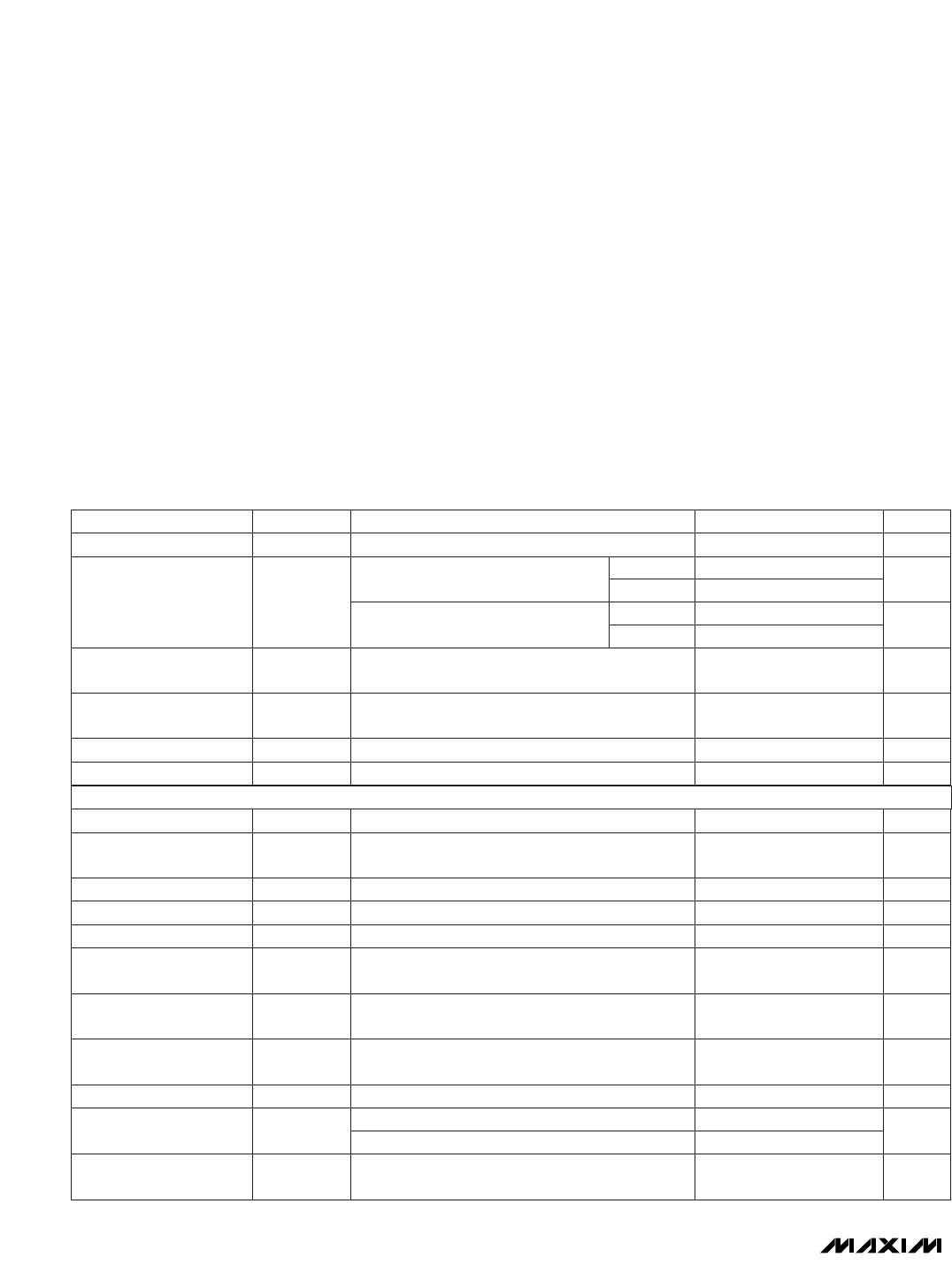
PART
MAX9000EUA
MAX9000ESA -40°C to +85°C
-40°C to +85°C
TEMP. RANGE PIN-PACKAGE
8 µMAX
8 SO
Ordering Information
Ordering Information continued at end of data sheet.
Rail-to-Rail is a registered trademark of Nippon Motorola, Ltd.
Pin Configurations and Typical Operating Circuit appear at
end of data sheet.
INTERNAL
PRECISION
REFERENCE
PIN-PACKAGE
MAX9000 Yes 8 SO/µMAX
MAX9001 Yes 10 µMAX, 14 SO
PART
MAX9002 No 8 SO/µMAX
OP-AMP GAIN
STABILITY
(V/V)
1
1
1
MAX9003 Yes 8 SO/µMAX
MAX9004 Yes 10 µMAX, 14 SO
MAX9005 No 8 SO/µMAX
10
10
10
SHUTDOWN
No
Yes
No
No
Yes
No
OP-AMP GAIN
BANDWIDTH
(MHz)
1.25
1.25
1.25
8
8
8
______________________________________________________________________________Selector Guide
MAX9001EUB
MAX9001ESD -40°C to +85°C
-40°C to +85°C 10 µMAX
14 SO
MAX9000–MAX9005
Low-Power, High-Speed, Single-Supply
Op Amp + Comparator + Reference ICs
2 _______________________________________________________________________________________
ABSOLUTE MAXIMUM RATINGS
ELECTRICAL CHARACTERISTICS
(V
DD
= +2.5V to +5.5V, V
SS
= 0, SHDN = V
DD
(MAX9001/MAX9004 only), V
CM(OP AMP)
= 0, V
AOUT
= V
DD
/ 2, V
CM(COMP)
= 0 (for
MAX9001/MAX9002/MAX9004/MAX9005), COUT = low, I
OUT(REF)
= 0, T
A
= T
MIN
to T
MAX
, unless otherwise noted. Typical values are
at V
DD
= 5V and T
A
= +25°C.)
Stresses beyond those listed under “Absolute Maximum Ratings” may cause permanent damage to the device. These are stress ratings only, and functional
operation of the device at these or any other conditions beyond those indicated in the operational sections of the specifications is not implied. Exposure to
absolute maximum rating conditions for extended periods may affect device reliability.
Supply Voltage (V
DD
to V
SS
)....................................-0.3V to +6V
Voltage Inputs (AIN_, CIN_).............(V
SS
- 0.3V) to (V
DD
+ 0.3V)
Output Short-Circuit Duration (AOUT, COUT, REF)...Continuous
to either V
SS
or V
DD
Continuous Power Dissipation (T
A
= +70°C)
8-Pin SO (derate 5.88mW/°C above +70°C).................471mW
8-Pin µMAX (derate 4.1mW/°C above +70°C)..............330mW
10-Pin µMAX (derate 5.6mW/°C above +70°C)............444mW
14-Pin SO (derate 8.3mW/°C above +70°C).................667mW
Operating Temperature Range
MAX900_E _ _...................................................-40°C to +85°C
Maximum Junction Temperature .....................................+150°C
Storage Temperature Range.............................-65°C to +160°C
Lead Temperature (soldering, 10sec).............................+300°C
V
SHDN
(0.3V x V
DD
), V
AOUT
= 0 to V
DD
Shorted to V
DD
Shorted to V
SS
MAX9000/MAX9001/
MAX9003/MAX9004
A
V
= 1V/V
V
DD
= 2.5V to 5.5V
MAX900_ES_, (V
SS
- 0.15V) V
CM
(V
DD
- 1.2V),
V
DD
= 5.5V
Guaranteed by PSRR tests
Guaranteed by CMRR test
Differential or common mode
MAX900_ES_
AIN+, AIN-
AIN+, AIN-
MAX9002/MAX9005
MAX9001/MAX9004 (V
SHDN
= 0)
MAX900_ES_
CONDITIONS
µA±0.01 ±1
I
OUT
(DISABLED)
Disabled Mode Output
Leakage
mA
65
Output Short-Circuit
Current
10
0.01Output Resistance
dB74 100PSRR
Power-Supply Rejection
Ratio
dBCMRR
Common-Mode
Rejection Ratio
72 96
V-0.15 V
DD
- 1.2CMVR
Input Common-Mode
Voltage Range
M1000R
IN
Input Resistance
nA±0.02 ±1Input Offset Current
nA±0.05 ±2I
BIAS
Input Bias Current
µV/°CTCV
OS
Input Offset Voltage
Temperature Coefficient
±1
µA
450 550
410 500
V2.5 5.5V
DD
Supply Voltage Range
V
OS
Input Offset Voltage mV±0.5 ±1.5
V0.3 x V
DD
V
IL(
SHDN
)
Shutdown Logic Low
340 425
µA
375 475
I
DD
Supply Current
µA2 5I
SHDN
Supply Current in
Shutdown
V0.7 x V
DD
V
IH(
SHDN
)
Shutdown Logic High
UNITSMIN TYP MAXSYMBOLPARAMETER
V
DD
= 3V
V
DD
= 5V
V
DD
= 3V
V
DD
= 5V
MAX9001/MAX9004 (V
SHDN
= 0 to V
DD
) µA1 2.5I
IN(
SHDN
)
Shutdown Input Bias
Current
OP AMP
MAX9000–MAX9005
Low-Power, High-Speed, Single-Supply
Op Amp + Comparator + Reference ICs
_______________________________________________________________________________________ 3
f = 10kHz
f = 10kHz
V
AIN+
- V
AIN-
10mV
V
DD
= 5.5V
V
DD
= 2.5V
CONDITIONS
fA/Hz
1I
NOISE
Input Noise Current Density
nV/Hz
36V
NOISE
Input Noise Voltage Density
pF2.5C
IN
Input Capacitance
140 250
1 5
1 5
94 125
dB
86 106
A
VOL
Large-Signal Voltage Gain
84 115
94 120
UNITSMIN TYP MAXSYMBOLPARAMETER
ELECTRICAL CHARACTERISTICS (continued)
(V
DD
= +2.5V to +5.5V, V
SS
= 0, SHDN = V
DD
(MAX9001/MAX9004 only), V
CM(OP AMP)
= 0, V
AOUT
= V
DD
/ 2, V
CM(COMP)
= 0 (for
MAX9001/MAX9002/MAX9004/MAX9005), COUT = low, I
OUT(REF)
= 0, T
A
= T
MIN
to T
MAX
, unless otherwise noted. Typical values are
at V
DD
= 5V and T
A
= +25°C.)
MAX9003/MAX9004/MAX9005
MAX9000/MAX9001/MAX9002
MHz
8
GBWGain-Bandwidth Product
1.25
mV
60 100
V
OL
/ V
OH
Output Voltage Swing
0.009
MAX9000/MAX9001/MAX9002
dB
30
degrees
75
µs2Power-On Time
µs2Enable Delay Time
µs0.2Shutdown Delay Time
MAX9000/MAX9001/MAX9002 (A
V
= 1V/V) 250
V
AOUT
= 0.05V to 2.45V, R
L
= 100k
V
AOUT
= 0.2V to 2.3V, R
L
= 1k
V
AOUT
= 0.05V to 5.4V, R
L
= 100k
V
AOUT
= 0.25V to 5.2V, R
L
= 1k
V
DD
- V
OH
V
OL
V
DD
- V
OH
V
OL
MAX9000/MAX9001/
MAX9002 (A
V
= 1V/V)
f = 10kHz,
V
AOUT
= 2Vp-p,
V
DD
= 5V
%
0.028
THD+N
Total Harmonic Distortion
plus Noise
MAX9003/MAX9004/
MAX9005 (A
V
= 10V/V)
V
DD
= 5V,
V
AOUT
= 4V step
µs
6.9
2.1
Settling Time to within 0.01%
MAX9000/MAX9001/
MAX9002 (A
V
= 1V/V)
MAX9003/MAX9004/
MAX9005 (A
V
= 10V/V)
MAX9003/MAX9004/MAX9005 (A
V
= 10V/V)
pF
250
C
LOAD
Capacitive-Load Stability
µV/°CTCV
OS
Input Offset Voltage
Temperature Coefficient
MAX900_ES_ ±1
mVInput-Referred Hysteresis V
DD
= 5V (Notes 2, 3) 4 7
R
L
= 100k
R
L
= 1k
MAX9003/MAX9004/MAX9005 80
Phase Margin
MAX9003/MAX9004/MAX9005 40
Gain Margin
mVV
OS
Input Offset Voltage MAX900_ES_ (Notes 1, 2) ±1 ±2
V
DD
= 5V,
V
AOUT
= 4V step
V/µs
0.85
6.0
SRSlew Rate
MAX9000/MAX9001/
MAX9002 (A
V
= 1V/V)
MAX9003/MAX9004/
MAX9005 (A
V
= 10V/V)
COMPARATOR

MAX9005EUA+T

Mfr. #:
Manufacturer:
Maxim Integrated
Description:
High Speed Operational Amplifiers Op Amp Comparator Reference IC
Lifecycle:
New from this manufacturer.
Delivery:
DHL FedEx Ups TNT EMS
Payment:
T/T Paypal Visa MoneyGram Western Union