MAX9000–MAX9005
Low-Power, High-Speed, Single-Supply
Op Amp + Comparator + Reference ICs
10 ______________________________________________________________________________________
_____________________________Typical Operating Characteristics (continued)
(V
DD
= +5V, V
SS
= 0, V
CM
(op amp) = 0, SHDN = V
DD
, COUT = low, R
L
= , T
A
= +25°C, unless otherwise noted.)
-2
-1
0
1
2
3
4
-2.0 -1.0-1.5 -0.5 0 0.5 1.0 1.5 2.0
V
REF
OUTPUT VOLTAGE CHANGE
vs. LOAD CURRENT
MAX9000 TOC46
LOAD CURRENT (mA)
V
REF
OUTPUT VOLTAGE CHANGE (mV)
SINKING
SOURCING
-100
-50
0
50
100
2.5 3.53.0 4.0 4.5 5.0 5.5
V
REF
OUTPUT VOLTAGE CHANGE
vs. SUPPLY VOLTAGE
MAX9000 TOC47
SUPPLY VOLTAGE (V)
V
REF
OUTPUT VOLTAGE CHANGE (µV)
50µs/div
V
REF
LOAD-TRANSIENT RESPONSE
I
OUT
2mA/div
V
REF
200mV/div
+1mA
-1mA
MAX9000-TOC48
5µs/div
V
REF
LINE-TRANSIENT RESPONSE
V
DD
500mV/div
V
REF
100mV/div
5.0V
4.5V
MAX9000-TOC49
500ns/div
MAX9000/MAX9001/MAX9002
OP-AMP SMALL-SIGNAL TRANSIENT RESPONSE
V
IN
50mV/div
V
OUT
50mV/div
MAX9000-TOC52
A
V
= +1
NO LOAD
1sec/div
V
REF
0.1Hz to 10Hz VOLTAGE NOISE
5µV/div
MAX9000-TOC50
100ns/div
-50mW
+50mW
COMPARATOR PROPAGATION DELAY
V
IN+
50mV/div
V
OUT
2V/div
V
IN
- = GND
NO LOAD
t
PD+
MAX9000-TOC51
t
PD-
1µs/div
MAX9000/MAX9001/MAX9002
OP-AMP SMALL-SIGNAL TRANSIENT
RESPONSE WITH C
LOAD
V
IN
50mV/div
V
OUT
50mV/div
MAX9000-TOC53
A
V
= +1
C
L
= 270pF
500ns/div
MAX9003/MAX9004/MAX9005
OP-AMP SMALL-SIGNAL TRANSIENT RESPONSE
V
IN
10mV/div
V
OUT
50mV/div
MAX9000-TOC54
A
V
= +10
NO LOAD
MAX9000–MAX9005
Low-Power, High-Speed, Single-Supply
Op Amp + Comparator + Reference ICs
______________________________________________________________________________________ 11
_____________________________Typical Operating Characteristics (continued)
(V
DD
= +5V, V
SS
= 0, V
CM
(op amp) = 0, SHDN = V
DD
, COUT = low, R
L
= , T
A
= +25°C, unless otherwise noted.)
Pin Description
Shutdown Logic Input 21
1µs/div
MAX9003/MAX9004/MAX9005
OP-AMP SMALL-SIGNAL TRANSIENT
RESPONSE WITH C
LOAD
V
IN
10mV/div
V
OUT
50mV/div
MAX9000-TOC55
A
V
= +1
C
L
= 270pF
2
µs/div
MAX9000/MAX9001/MAX9002
OP-AMP LARGE-SIGNAL TRANSIENT RESPONSE
V
IN
5V/div
4V
0V
V
OUT
1V/div
MAX9000-TOC56
A
V
= +1
NO LOAD
500ns/div
MAX9003/MAX9004/MAX9005
OP-AMP LARGE-SIGNAL TRANSIENT RESPONSE
V
IN
0.5V/div
5V
0V
V
OUT
1V/div
MAX9000-TOC57
A
V
= +10
NO LOAD
MAX9000/
MAX9003
FUNCTION
MAX9002/
MAX9005
SHDN
32 AOUT Op-Amp Output11
43 AIN-
54 AIN+ Noninverting Op-Amp Input33
Inverting Op-Amp Input22
65 V
SS
96 REF Internal Reference Output5
107 CIN-
118 CIN+ Noninverting Comparator Input66
Inverting Comparator Input5
Negative Supply or Ground44
129 COUT Comparator Output77
1310 V
DD
1, 7, 8, 14 N.C. No Connection. Not internally connected.
Positive Supply88
NAME
PIN
MAX9001/MAX9004
10 µMAX 14 SO
MAX9000–MAX9005
Low-Power, High-Speed, Single-Supply
Op Amp + Comparator + Reference ICs
12 ______________________________________________________________________________________
_______________Detailed Description
The MAX9001–MAX9005 are combinations of a high-
speed operational amplifier, a 185ns comparator, and a
1%-accurate, 8ppm/°C, 1.230V reference. The devices
are offered in space-saving 8-pin and 10-pin µMAX pack-
ages. The comparator’s inverting input is internally con-
nected to the reference output in the MAX9000/MAX9003.
The MAX9002/MAX9005 do not have an internal refer-
ence, but the inverting input of the comparator is avail-
able externally. The MAX9001/MAX9004 include both the
inverting input and the reference output. The MAX9000/
MAX9001/MAX9003/MAX9004 typically consume only
410µA of quiescent current, while the MAX9002/
MAX9004 typically consume 340µA. These low-power,
Rail-to-Rail devices provide excellent AC and DC perfor-
mance and are ideally suited to operate from a single
supply. The MAX9001/MAX9004 feature a shutdown
mode that sets the outputs in a high-impedance state and
reduces the supply current to 2µA, making these devices
ideal for portable and battery-powered systems.
Op Amp
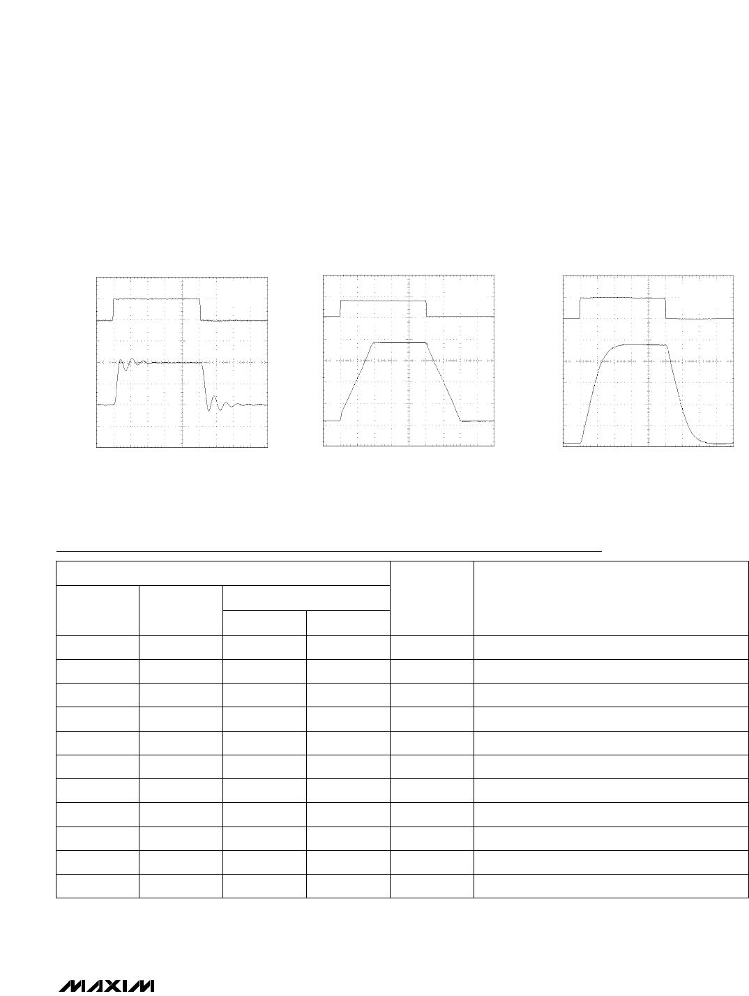
The op amps in the MAX9000/MAX9001/MAX9002 are
unity-gain stable with a gain-bandwidth product of
1.25MHz and a slew rate of 0.85V/µs. The amplifiers in
the MAX9003/MAX9004/MAX9005 are stable at closed-
loop gains greater than or equal to 10V/V, with a gain-
bandwidth product of 8MHz and a slew rate of 6.0V/µs.
The common-mode input voltage range extends from
150mV below the negative rail to within 1.2V of the pos-
itive rail. The amplifier output does not undergo phase
reversal when the common-mode input range is
exceeded, and the input impedance is relatively con-
stant for input voltages within both supply rails. The
MOS differential inputs of the amplifiers feature
extremely high input impedance and ultra-low input
bias currents. The CMOS output stage achieves true
rail-to-rail operation; the outputs swing to within a few
millivolts of the supply rails, thus extending the dynamic
range. A proprietary design achieves high open-loop
gain, enabling these devices to operate at low quies-
cent currents yet maintain excellent DC and AC char-
acteristics under various load conditions. These
devices have been designed to maintain low offset volt-
age over the entire operating-temperature, common-
mode, and supply-voltage ranges.
MAX9000
MAX9003
OP AMP
COMP
REF
1
2
3
4
8
7
6
5
AOUT
AIN-
AIN+
V
SS
V
DD
COUT
CIN+
REF
MAX9002
MAX9005
OP AMP
COMP
1
2
3
4
8
7
6
5
AOUT
AIN-
AIN+
V
SS
V
DD
COUT
CIN+
CIN-
MAX9001
MAX9004
OP AMP
COMP
REF
4M
3
4
5
6
12
11
10
9
AOUT
AIN-
AIN+
V
SS
V
DD
2 13SHDN V
DD
CIN+
CIN-
REF
NORMAL/SHUTDOWN CONTROL
Figure 1. MAX9000–MAX90005 Functional Diagrams

MAX9005EUA+T

Mfr. #:
Manufacturer:
Maxim Integrated
Description:
High Speed Operational Amplifiers Op Amp Comparator Reference IC
Lifecycle:
New from this manufacturer.
Delivery:
DHL FedEx Ups TNT EMS
Payment:
T/T Paypal Visa MoneyGram Western Union