Comparator
The common-mode input range extends from 150mV
below the negative rail to within 1.1V of the positive rail.
The bipolar differential inputs of the comparator feature
high input impedance and low input bias currents. The
comparators are designed to maintain low offset volt-
age over the entire operating-temperature, common-
mode, and supply-voltage ranges. In the MAX9000/
MAX9003, the comparator’s inverting input is internally
connected to the reference output.
The CMOS output stage achieves true rail-to-rail opera-
tion; the outputs swing to within a few millivolts of the
supply rails. The comparator’s propagation delay is
185ns and is a function of the overdrive (see
Typical
Operating Characteristics
). TTL/CMOS compatibility is
maintained even with a ±4mA output load. A propri-
etary design of the output stage substantially reduces
the cross-conduction current during output transitions,
thereby minimizing power-supply glitches typical of
most comparators. In addition, the comparator’s ±2mV
of built-in hysteresis provides noise immunity and pre-
vents unstable outputs even with slow-moving input
signals.
Voltage Reference
The 1%-accurate, precision 1.230V internal bandgap
reference in the MAX9000/MAX9001/MAX9003/
MAX9004 achieves an 8ppm/°C temperature coefficient
(tempco). The reference can sink or source 1mA of load
current with excellent load regulation. The output typical-
ly changes only 60µV for a 3V change in input voltage
(line regulation). The reference is stable for capacitive
loads up to 100nF.
Applications Information
The MAX9000–MAX9005 offer excellent performance
and low power consumption, and are available in
space-saving µMAX packages. The following section
provides some practical application guidelines.
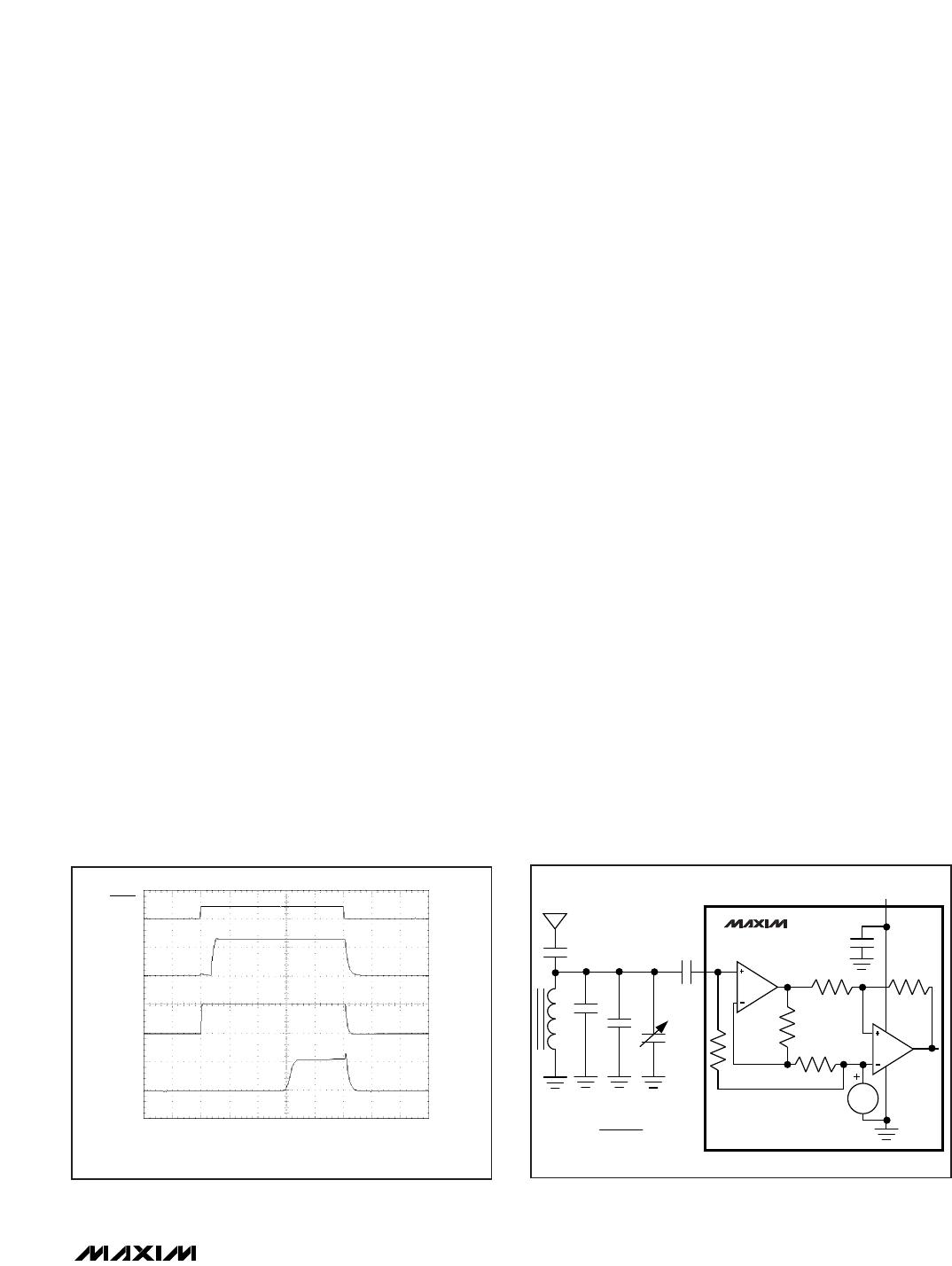
Bypassing and Layout
The MAX9000–MAX9005 operate from a +2.5V to +5.5V
single supply or from ±1.25V to ±2.75V dual supplies.
(In the MAX9000/MAX9001/MAX9003/MAX9004, the
reference voltage is referred to as V
SS
.). For single-
supply operation, bypass the power supply with a
0.1µF capacitor. For dual supplies, bypass each supply
to ground. Bypass with capacitors as close as possible
to the device to minimize lead inductance and noise.
Use a low-inductance ground plane if possible. A print-
ed circuit board with a ground plane is recommended.
Avoid using wire-wrap boards, breadboards, or IC
sockets. For heavy loads at the comparator’s and/or
amplifier’s output, add a 1µF to 10µF power-supply
bypass capacitor.
The device has a high degree of isolation between the
various blocks. To maintain isolation, careful layout is
required. Take special precautions to avoid crossing
signal traces, especially from the outputs to the inputs.
For sensitive applications, shielding might be required.
In addition, stray capacitance may affect the stability
and frequency response of the amplifier. Decrease
stray capacitance by minimizing lead lengths in the
board layout, as well as placing external components
as close to the device as possible.
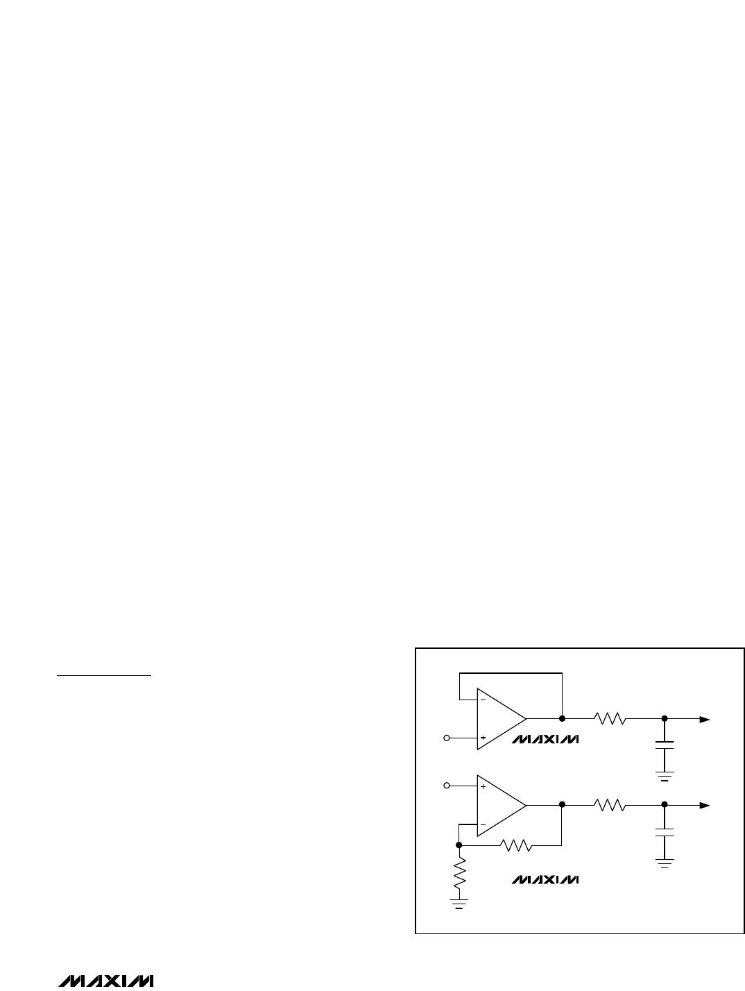
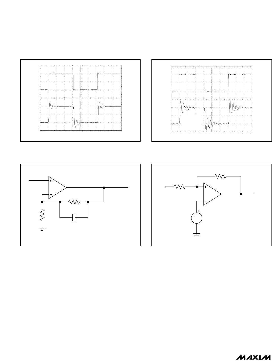
Op-Amp Frequency Stability
Driving large capacitive loads can cause instability in
most low-power, rail-to-rail output amplifiers. These
amplifiers are stable with capacitive loads up to 250pF in
their minimum gain configuration. Stability with higher
capacitive loads can be improved by adding an isolation
resistor in series with the op-amp output, as shown in
Figure 2. This resistor improves the circuit’s phase mar-
gin by isolating the load capacitor from the amplifier’s
output. Figures 3 and 4 show the response of the ampli-
fier with and without an isolation resistor, respectively.
The total capacitance at the op amp’s inputs (input
capacitance + stray capacitance) along with large-value
feedback resistors can cause additional poles within the
amplifier’s bandwidth, thus degrading the phase margin.
To compensate for this effect, place a 2pF to 10pF
capacitor across the feedback resistor, as shown in
Figure 5.
MAX9000–MAX9005
Low-Power, High-Speed, Single-Supply
Op Amp + Comparator + Reference ICs
______________________________________________________________________________________ 13
MAX9000
MAX9001
MAX9002
MAX9003
MAX9004
MAX9005
R
S
R
R
R
S
C
LOAD
C
LOAD
Figure 2. Isolation Resistors to Drive Capacitive Loads
MAX9000–MAX9005
Reference Bypassing
While the internal reference is stable with capacitive
loads up to 100nF, it does not require an output capaci-
tor for stability. However, in applications where the load
or the supply could experience large step changes, an
output capacitor reduces the amount of overshoot and
improves the circuit’s transient response.
Comparator Input Stage
The comparator’s input bias current is typically 8nA. To
reduce the offset error caused by the bias current flow-
ing through the external source impedance, match the
effective impedance seen by each input. High source
impedance together with the comparator’s input capaci-
tance can increase the propagation delay through the
comparator. The outputs do not undergo phase rever-
sal when the input common-mode range is exceeded,
and the input impedance is relatively constant for input
voltages within both supply rails.
Comparator Hysteresis
Built-in ±2mV hysteresis improves the comparator’s
noise immunity. It prevents unstable outputs with slow-
moving or noisy input signals. If additional hysteresis is
required, add positive feedback as shown in Figure 6.
This configuration increases the hysteresis band to
desired levels, but also increases power consumption
and slows down the output response.
Low-Power, High-Speed, Single-Supply
Op Amp + Comparator + Reference ICs
14 ______________________________________________________________________________________
2µs/div
V
IN
50mV/
div
V
OUT
50mV/
div
MAX9000-FIG03
Figure 3. MAX9000/MAX9001/MAX9002 Op-Amp Small-Signal
Transient Response with Capacitive Load (C
L
= 510pF) and
Isolation Resistor (R
ISO
= 91
)
Figure 5. Compensation for Input Capacitance
R1
R2
2pF TO 10pF
AOUT
AIN+
2µs/div
V
IN
50mV/
div
V
OUT
50mV/
div
MAX9000-FIG04
V
DD
= +1
C
L
= 510pF
Figure 4. MAX9000/MAX9001/MAX9002 Op-Amp Small-Signal
Transient Response with Capacitive Load (C
L
= 510pF) and
No Isolation Resistor
REF
R2
R1
COUT
V
IN
Figure 6. External Hysteresis
To add hysteresis, use the following procedure:
Step 1: The device’s input bias current can be as high
as 80nA. To minimize error due to the input bias,
choose a value for R2 of 100k(V
REF
/ R2), which
allows a current of 12.33µA at the upper trip point.
Step 2: Choose the width of the hysteresis band. In this
example, choose 20mV for the added external hystere-
sis (V
EHYST
= 20mV). Total hysteresis = V
EHYST
+
V
IHYST
= 24mV.
R1 = R2 (V
EHYST
- 2V
IHYST
) / (V
DD
+ 2V
IHYST
)
where
IHYST
is the device’s internal hysteresis.
Step 3: Determine R1. If V
DD
= 5V, then R1 = 319.
Step 4: Check the hysteresis trip points. The following
equation represents the upper trip point (V
IN(H)
):
V
IN(H)
= [(R1 + R2) / R2] (V
REF
+ V
IHYST
) = 1.238V
The lower trip point is 24mV lower than upper trip point.
V
IN(L
)
= 1.238V - 0.024V = 1.214V.
Comparator Propagation Delay
The comparator’s propagation delay is a function of the
input overdrive voltage. Overdrive voltage is measured
from beyond the edge of the offset and hysteresis-
determined trip points (see
Typical Operating
Characteristics
for a graph of Propagation Delay vs.
Input Overdrive). High source impedance coupled with
the comparator’s input capacitance increases the prop-
agation delay. Large capacitive loads also increase the
propagation delay.
Shutdown
(
SSHHDDNN
)
Shutdown is active-low enabled. The SHDN input for
the MAX9001/MAX9004 can be taken above the posi-
tive supply without an increase in the SHDN input cur-
rent, allowing them to be driven from independent logic
circuits powered from a different supply voltage.
However, the logic threshold voltage requirements
must be met for proper operation. If SHDN is left
unconnected, the device defaults to the enabled mode
through an internal 4Mpull-up to V
DD
. If SHDN is to
be left unconnected, take proper care to ensure that no
signals are coupled to this pin, as this may cause false
triggering.
In shutdown mode, all outputs are set to a high-imped-
ance state and the supply current reduces to 2µA.
Enable times for the op amp, comparator, and refer-
ence are 2µs, 100ns, and 16µs, respectively. Shutdown
delay times for the op amp, comparator, and reference
are 200ns, 100ns, and 1µs, respectively (Figure 7).
________________Application Circuits
Radio Receiver for Alarms
and Detectors
Figure 8’s circuit is useful as a front end for RF alarms.
An unshielded inductor is used with capacitors C1A,
C1B, and C1C in a resonant circuit to provide frequen-
cy selectivity. The op amp from a MAX9003 amplifies
the signal received. The comparator improves noise
immunity, provides a signal-strength threshold, and
translates the received signal into a pulse train. The
tuned LC circuit in Figure 8 is set for 300kHz. The lay-
out and routing of components for the amplifier should
be tight to minimize 60Hz interference and crosstalk
from the comparator. Metal shielding is recommended
to prevent RFI from the comparator or digital circuitry
from exciting the receiving antenna. The transmitting
MAX9000–MAX9005
Low-Power, High-Speed, Single-Supply
Op Amp + Comparator + Reference ICs
______________________________________________________________________________________ 15
5µs/div
SHDN
5V/div
AOUT
2V/div
COUT
5V/div
VREF
1V/div
MAX9000-FIG07
A
V
= +1V/V, C
AIN+
= 2.5V, C
CIN+
= 2.5V
Figure 7. Enable/Disable Response of Op Amp, Comparator,
and Reference to
SHDN
REF
0.1µF
0.1µF
L1
33µH
C1A
390pF
1
(2π f
C
)
2
C1B
0.01nF
C1C
10M
5.1M
9.1k
10k
1.230V
20k
V
CC
= 5V
COMP
ANTENNA
AMP
LAYOUT-SENSITIVE AREA,
METAL RFI SHIELDING ADVISED
MAX9003
L1 x C1 =
50-100pF
Figure 8. Radio Receiver Application

MAX9005EUA+T

Mfr. #:
Manufacturer:
Maxim Integrated
Description:
High Speed Operational Amplifiers Op Amp Comparator Reference IC
Lifecycle:
New from this manufacturer.
Delivery:
DHL FedEx Ups TNT EMS
Payment:
T/T Paypal Visa MoneyGram Western Union